The pace of semiconductor development in the last few decades has been nothing short of incredible. Every year, there’s a new "world’s fastest CPU," a denser, faster RAM module, sensors that can detect a whisper of a change in the environment, and power converters that sip current instead of guzzling it. It’s an arms race — and if you’re reading this, you’re probably as invested in it as I am.
But here’s the blunt truth: while the semiconductor devices themselves are evolving at breakneck speed, the packages we cram them into are still lagging behind. We’re putting hypercars into cardboard boxes and acting surprised when the performance isn't perfect.
Sure, there have been important developments — System-on-Chip (SoC) designs being one of the most noteworthy. SoCs have absolutely transformed mobile and embedded systems, allowing us to shrink whole boards into fingernail-sized marvels. Without them, modern smartphones, smartwatches, and IoT devices wouldn't exist as we know them.
But let's not pretend SoCs are a silver bullet. They come with their own basket of issues. For starters, discrete devices — good old-fashioned individual chips — are often easier to manufacture, easier to source, and are tailor-made to slip neatly into existing PCB manufacturing processes. When you’re managing high-volume production or designing rugged industrial systems, discrete still reigns supreme.
The downside? Size and complexity. Discrete-based designs sprawl across a board like an overambitious city plan. They’re simply too big and unwieldy for applications where compactness is non-negotiable — like mobile devices, wearables, and certain classes of industrial IoT nodes. In the world of portability, the bloated footprint of discrete circuits is a non-starter.
Enter the SoC. Perfect for compact devices, indispensable for anything IoT. But even the mighty SoC has hard limitations. One of the dirty little secrets of SoCs is that they often can't fully capitalize on the very latest semiconductor process nodes. There's a lag — because bringing an SoC to a bleeding-edge node costs an astronomical amount of money and risk, meaning they usually trail behind discrete devices built on newer processes.
Another huge hurdle is the third dimension — or, more accurately, the lack of it. SoCs largely live in the X-Y plane. They spread out flat on the PCB, and that's about it. Stacking, true 3D integration, remains the domain of more exotic (and far more expensive) technologies like 3D ICs and advanced packaging methods that most SoCs simply don’t tap into. That leaves SoC designs needing a healthy diet of external support components — power management ICs, RF front ends, memory modules — to be practically useful.
And the result? Even with an SoC, your "compact" design can balloon into something far bigger than you intended once all those necessary externals are factored in.
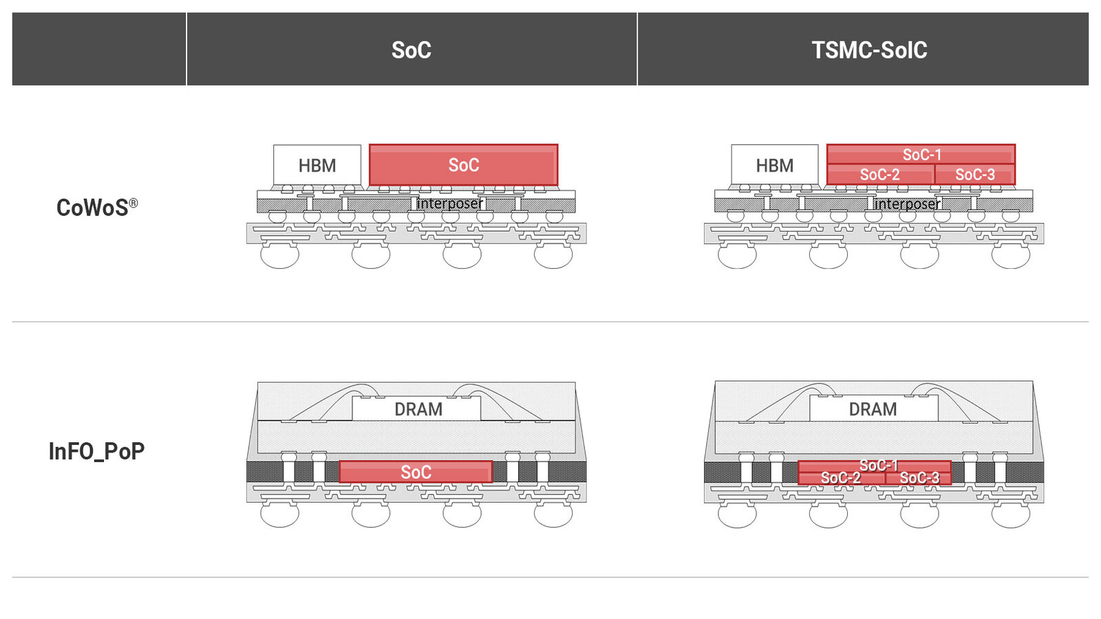
TSMC, a Taiwanese semiconductor manufacturer, is reportedly experiencing rapid growth in its SoIC (system-on-integrated-chip) packaging technology, with some attributing this success to the increased demand from Apple and AMD. According to a recent report from Economic News Daily, TSMC has seen a significant increase in orders for SoIC packaging, which is expected to continue through the end of 2024.
SoIC packaging is a relatively new technology that combines all system components onto a single silicon die. This design enables for increased performance, efficiency, and reduced latency compared to traditional packaging methods. TSMC has been at the forefront of this technology, and its rapid growth is expected to continue as more companies adopt this advanced packaging solution.
Apple is one of the major customers of TSMC, and it has been reported that the iPhone maker is considering the use of SoIC technology in its next-generation chipsets. Specifically, Apple is expected to adopt SoIC packaging for the higher-tier versions of the M5 chip, which will be used in the updated 14-inch and16-inch MacBook Pro models later this year. The base model of the M5 chip will not utilize this technology, but the M5 Pro and higher-end variants are expected to take advantage of it.
AMD is another major customer of TSMC, with the semiconductor manufacturer reportedly producing millions of AMD chips per month. While AMD has not publicly announced plans to use SoIC technology, it is likely that the company will follow Apple's lead in adopting this advanced packaging solution.
NVIDIA has also been mentioned as a potential customer for TSMC's SoIC technology. The graphics chip titan is expected to use the SoIC technology in its Rubin architecture, but it is unclear whether NVIDIA has already placed orders for the technology. TSMC is shifting its focus from CoWo (chip on wafer on substrate) to SoIC technology, as its customers prefer to showcase their next-generation offerings using this advanced packaging solution.
With TSMC’s aggressive development of SoIC technology, it's clear that SoICs aren't some pie-in-the-sky academic experiment — they're rapidly becoming a commercial reality. The question isn't if SoICs will have an impact. It's how big that impact will be.
The truth is, while SoIC designs are inherently more complex than traditional layouts, they might be exactly the innovation that embedded systems design has been desperately waiting for. We’re reaching the limits of what can be crammed into two dimensions. Boards can only get so crowded before they become a nightmare of compromises — in routing, power, thermal management, and even reliability. SoICs offer a different path forward: finally making serious use of the third dimension.
By stacking SoCs on top of other SoCs, designers can dramatically increase functionality without blowing up the X-Y footprint. And considering how razor-thin modern dies are — we’re talking about structures measured in microns — multiple layers could be stacked with barely any noticeable increase in vertical height. You’re not building a skyscraper; you’re adding a few sheets of paper. The end result? Devices that are orders of magnitude more powerful, packed into the same physical footprint as their last-generation counterparts.
Of course, there are major technical hurdles, notably in heat removal and power distribution. Stack enough high-performance dies together and you’re effectively creating a tiny thermal bomb. Managing that heat without sacrificing performance is a non-trivial engineering challenge — and I don’t buy the hand-waving some people do around it. The same goes for efficiently distributing clean, stable power across multiple layers of active silicon.
But here’s the reality: these are solvable problems. The semiconductor industry has tackled tougher challenges before, and if the demand (read: money) is there, solutions will be found — whether through new materials, novel cooling techniques, or smarter architectural designs.
Personally, I’m excited about SoIC. Genuinely. This isn't another "bendable screen" gimmick or a half-baked "smart" coffee maker. This is the kind of foundational change that could completely redefine embedded and mobile design.
For now, though, all we can do is sit back, watch the developments closely, and — if you’re smart — start thinking about how your future designs might leverage SoIC when it becomes widely available. Because one thing's for certain: the landscape is about to change, and you’ll want to be ready for it.