Ask anyone outside the field what drives progress in electronics, and they’ll probably parrot back something about faster processors or shrinking transistors — the classic Moore’s Law narrative. And yes, those improvements are real, necessary, and impressive. But they’re also only half the story. The truth is, there are foundational technologies quietly evolving in the background that deserve just as much attention. Chief among these are connectors and PCBs — the literal glue and ground on which modern electronics are built.
Let’s start with connectors. No one gets excited about them, but they should. Connectors are the veins and arteries of every system — without them, you're left with nothing but isolated components and frustrated engineers. Companies like Omnetics and Samtec (you’ve probably handled one of their parts without realizing it) are doing remarkable work here. Whether it’s ultra-high-speed board-to-board interconnects or micro-pitch cable assemblies that can survive vibration, temperature swings, and time itself — the progress in this space is nothing short of surgical-grade engineering.
But the unsung hero of all this innovation is the printed circuit board. It doesn’t boot your OS, but it sure as hell decides if your device ever gets that far. The PCB industry has been undergoing a constant transformation ever since their introduction, and not enough people are talking about it.
Modern PCBs are not just green rectangles with copper traces. They’re high-frequency signal highways, thermal management solutions, and mechanical backbones all rolled into one. We’re now seeing microvias smaller than the thickness of a human hair, and HDI (High-Density Interconnect) boards that can pack more functionality per square centimeter than most full-sized computers from the early 2000s. Want faster clock speeds and larger memory capacities? You don’t get there without this kind of substrate-level innovation.
Then there are material advances. FR-4 is still common, but increasingly being replaced or augmented with advanced laminates like Rogers and Teflon-based materials for high-speed digital and RF applications. These new materials reduce signal loss, improve impedance control, and allow for better thermal performance — which directly translates into longer product life and better reliability. Not flashy, but critical.
And let’s not forget the assembly side. New soldering techniques — from selective soldering to laser reflow — are opening doors for more compact and irregular form factors. This is enabling things like wearable medical devices, ultra-compact IoT sensors, and even electronics embedded into textiles. It’s all very sci-fi, but it’s happening now, and PCBs are at the core of it.
So yes, smaller transistors are impressive. But if we’re being honest, it's the less glamorous layers — the connectors, the PCBs, the solder joints — that hold the real power to enable innovation. They’re not always headline material, but without them, the rest wouldn’t work.
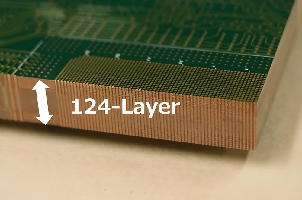
In a significant advancement for the electronics industry, OKI Circuit Technology (OTC), a leading printed circuit board (PCB) manufacturer, (has successfully developed a new 124-layer PCB technology)[https://www.oki.com/global/press/2025/04/z25006e.html]. This achievement represents a 15% increase in layer count over conventional 108-layer PCBs, setting a new benchmark for the industry.
The new technology has been specifically designed for wafer inspection equipment used in the production of next-generation high bandwidth memory (HBM) chips. These high-performance memory modules are essential for enabling advanced artificial intelligence (AI) applications, which require rapid data processing and high-speed data transmission between graphics processing units (GPUs) and memory. The HBM technology utilized in these applications features a stacked DRAM structure, necessitating the development of advanced PCBs that can handle the increased complexity and density of these components.
To achieve the 124-layer design, OTC employed ultra-thin materials and proprietary tools, along with the development of a unique automatic transport system for handling these materials. The new technology has been successfully demonstrated in a 7.6 mm thick PCB, representing a significant advancement in PCB manufacturing capabilities.
The development of 124-layer PCBs is a crucial step towards enabling the widespread adoption of next-generation AI semiconductors and other high-performance applications. The increased layer count and thinner material thickness will enable the creation of more complex and compact PCBs, driving advancements in fields such as aerospace, defense, robotics and next-generation communications. OTC plans to establish mass production capabilities for the new technology by October 2024 at its Joetsu plant in Niigata Prefecture.
The success of the 124-layer PCB technology has been recognized by industry experts, who acknowledge the significant impact it will have on the electronics industry. The ability to increase the layer count and density of PCBs will enable the creation of smaller, faster, and more powerful electronic devices, driving innovation and growth in various sectors.
In recognition of this achievement, OTC will be showcasing the new technology at the upcoming PCB East 2025 conference in Massachusetts, USA. The exhibition, scheduled for April 30 to May, 2025, will provide a platform for industry professionals to learn about the latest advancements in PCB manufacturing and explore opportunities for collaboration and innovation.
Let’s not get carried away. While the engineering behind OKI’s 124-layer PCB is undeniably impressive, it’s not about to show up in your next smartwatch or smart toaster. At 7.6 mm thick, it might not sound like much, but in the world of consumer electronics — where every tenth of a millimeter counts — this is a chunky, premium-grade slab of infrastructure.
These boards are not designed for the average application. They're tailored for high-speed systems, ultra-dense interconnects, and mission-critical signal integrity. Think wafer inspection machines, defense hardware, space systems, and maybe, just maybe, some ultra-high-end AI servers. Your average laptop? Not a chance. Even your $2,000 smartphone isn’t squeezing in anything remotely this complex.
And that’s not just because of the size. The construction method is a whole other level of exotic. We're talking about custom ultra-thin materials, specialized layering processes, and automatic transport systems — this isn’t your garden-variety PCB fab house running a few extra lamination cycles. It’s custom manufacturing for a niche class of electronics.
In fact, for 99% of designs, if you can’t get it done with a 4-layer board, you’re likely over-engineering, or you’ve taken a wrong turn somewhere in your architecture. Six layers? Sure, if you're juggling signal integrity or power planes. Eight? Fine for denser routing. But beyond that? You’re deep into speciality territory.
That said, we’re witnessing the absolute frontier of what PCBs can become. And just like everything in electronics, today's luxury often becomes tomorrow’s standard. It’s unlikely we’ll see 124 layers in consumer tech anytime soon, but the techniques used to build these boards — tighter layer registration, advanced materials, smarter stacking methods — could trickle down and reshape how we design mid-range PCBs in the next five to ten years.
So no, your next Arduino project won’t be rocking 124 layers — and it really, really shouldn’t. But it’s still exciting to imagine where this capability could lead. AI inference hardware in edge devices? Satellite control systems the size of a deck of cards? It opens up design possibilities that were science fiction a decade ago.
This is one of those "just because you can doesn’t mean you should" technologies — but I, for one, am glad someone did.