AOS Backs NVIDIA’s 800 VDC Power Architecture With SiC and GaN for Next-Generation AI Factories
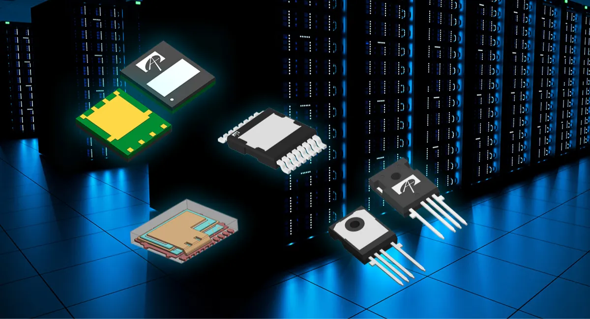 The move toward AI factories has pushed data center power architecture to a breaking point. NVIDIA’s shift from the familiar 54 V distribution model to a new 800 VDC system marks one of the largest transitions the industry has seen in years. It changes everything from rack construction to conversion stages, and it places new demands on the power semiconductors that support the entire system. Alpha and Omega Semiconductor (AOS) has announced a portfolio of SiC, GaN, MOSFET and controller technologies aimed directly at these requirements, positioning the company as an early contributor to this new high-voltage landscape.
Why the Move to 800 VDC Matters
AI infrastructure is now defined by megawatt-scale racks, high-density GPU clusters and power delivery networks pushed close to their physical limits. Traditional 54 V distribution works, but it is starting to constrain system efficiency, copper use and long-distance distribution inside large facilities. NVIDIA’s 800 VDC architecture is an attempt to break through these limitations. Higher voltage means lower current for the same power transfer, and that reduces conduction losses, cable size and conversion overheads. It also opens the door to simpler AC-to-DC front ends, with fewer cascaded stages and less thermal stress across the system.
These gains only work if the power devices handling the 800 VDC bus can switch quickly, survive high temperatures, and maintain low losses under heavy load. This is where SiC and GaN become essential. AOS is positioning its latest wide bandgap portfolio as building blocks for each stage of the new power delivery chain.
Supporting High-Voltage Front Ends With SiC
The first step in NVIDIA’s proposed architecture is high-voltage AC-to-DC conversion at the facility perimeter. AOS highlights devices such as the AOM020V120X3 and the topside-cooled AOGT020V120X2Q for this stage. These are 1200 V SiC MOSFETs designed for high efficiency under large voltage swings and elevated switching frequencies. Their role is to collapse incoming grid power, often around 13.8 kV, into a stable 800 VDC rail with fewer intermediate conversions. This reduces system complexity, improves fault tolerance and cuts cumulative losses. SiC is particularly well suited here because of its ability to handle high voltage and temperature without compromising switching speed.
GaN for High-Density Rack-Level Conversion
Once power reaches the rack, the challenge shifts toward density. AI compute modules need local converters that can quickly bring 800 V down to intermediate rails before reaching GPU and accelerator modules. AOS targets this part of the chain with GaN switches such as the upcoming AOGT035V65GA1 and the AOFG018V10GA1. GaN’s fast switching capability allows designers to shrink magnetics and capacitors, which frees up real estate inside rack power modules. Faster switching also means tighter regulation and lower ripple, both of which matter when feeding high-performance computing silicon.
The benefit is not only size reduction. GaN’s efficiency helps keep thermal load under control, which has become one of the biggest constraints in racks filled with multi-kilowatt GPU servers.
Packaging and Secondary Conversion Flexibility
For the secondary side of LLC converters and the final steps of stepping down to 12 V and below, AOS offers stacked-die MOSFETs such as the AOPL68801. These share footprint compatibility with the company’s 100 V GaN FETs, giving engineers the option to adjust cost, performance and density without redesigning the board. This level of flexibility is useful when multiple converter topologies must coexist across large systems, each with its own efficiency targets and thermal budget.
Multi-Phase Control for AI SoCs
The last stage in the chain sits inches away from the GPU and AI SoCs. AOS’ multi-rail, 16-phase controllers support the conversion from intermediate voltages down to the low voltages required by large accelerator dies. These controllers manage transients, maintain tight voltage accuracy and respond quickly to dynamic loading, all of which are essential for modern AI workloads that fluctuate between idle and peak compute in milliseconds.
Implications for AI Factory Design
The shift to 800 VDC architecture is not a minor optimisation. It affects electrical safety design, cabling strategies, rack topologies and cooling systems. AOS’ portfolio highlights how much semiconductor innovation is required to support this transition. With the right combination of SiC for high-voltage conversion, GaN for density, and advanced MOSFETs and controllers for local regulation, data center designers can reduce copper usage, improve end-to-end efficiency and lower the cooling burden inside high-power racks.
Industry estimates suggest gains of up to five percent in overall efficiency and significant reductions in copper usage. In large AI facilities consuming tens of megawatts, these gains accumulate rapidly and translate into lower operational cost and higher compute density.
As AI factories continue to scale, the move toward higher-voltage distribution looks increasingly unavoidable. AOS’ involvement in early support for the 800 VDC model shows how power semiconductor suppliers are adapting to meet the needs of a new era of data center design, one defined by higher power, greater density and an escalating demand for efficiency at every step of the power path.
Learn more and read the original article on www.aosmd.com
You may also like