Alpha and Omega’s 600V αMOS E2 Device Targets High Stress Power Designs
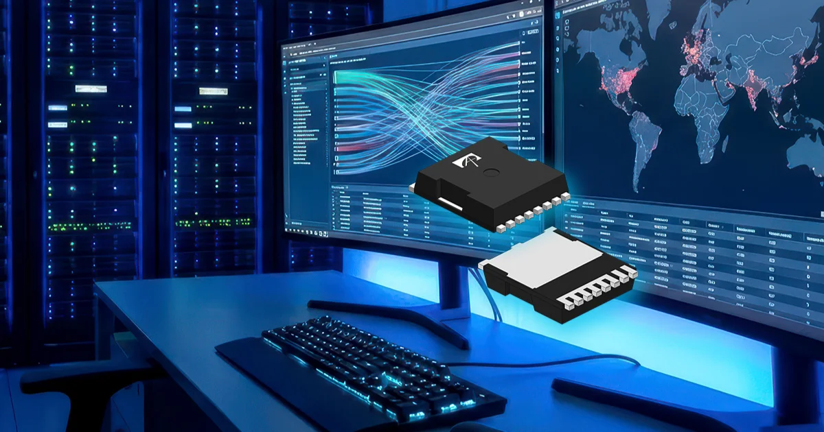 Engineers building modern power stages know how much stress the high-voltage switch needs to absorb when servers, solar inverters, or industrial drives push for tighter efficiency and higher density. Thermal margins shrink, switching transitions become sharper, and reliability expectations climb at the same time. Alpha and Omega Semiconductor’s new αMOS E2 platform steps directly into that space. The first device out of the platform, the 600 V AOTL037V60DE2, arrives with a focus on handling the real electrical abuse that high power stages see in practice rather than just meeting static datasheet values.
A Platform Built Around Real Switching Stress
What makes this generation relevant is the way AOS has shaped the device for the topologies that dominate mid to high power designs. Systems built around totem pole PFC, LLC tanks, and phase shifted bridges have to maintain efficiency while managing fast transitions and tight control loops. A common challenge is the stress placed on the body diode during abnormal events. When diodes reverse recover under load or when start-up conditions spike the current, devices can see conditions that fall well outside the steady-state operating region. AOS designed the αMOS E2 structure to tolerate those events without compromising conduction or switching behavior in normal operation.
Body Diode Behavior That Supports Abnormal Events
One detail worth noting is how much attention AOS gives to the intrinsic diode. Reverse recovery performance is often the differentiator between a system that rides through a transient and one that fails in the field. The AOTL037V60DE2 showed the ability to handle a di/dt of 1300 A per microsecond at a junction temperature of 150 degrees Celsius under specific forward current conditions. That level of diode ruggedness is significant because it allows engineers to keep their magnetic and protection design stable without relying on unusual snubbers or clamp networks. In practice this can simplify both layout and mechanical design when the power stage is packed tightly inside a chassis.
Electrical Characteristics Shaped for High Density Stages
The device arrives in a TOLL package with a maximum on resistance of 37 milliohms. For engineers running high power density stages, the combination of conduction performance and switching behavior is what sets the tone for thermal design. AOS reports that the αMOS E2 device maintained strong Avalanche Unclamped Inductive Switching performance and extended short circuit withstanding time when compared with competing MOSFETs. These characteristics matter because real systems are rarely perfectly controlled. Motors stall, converters misfire during tuning, and solar inverters hit non ideal load steps. A MOSFET that can tolerate those edges provides headroom that extends beyond efficiency figures.
Reliability Considerations for Next Generation Power Platforms
As power architectures continue to push toward higher frequency switching and denser mechanical layouts, reliability becomes more difficult to maintain. The combination of diode robustness, avalanche capability, and short circuit tolerance positions the AOTL037V60DE2 as a device that supports these shifts without forcing major system redesigns. For engineers balancing the competing needs of efficiency, thermal management, and cost, this kind of high voltage device can reduce the number of protective elements needed in the system. The takeaway is that the αMOS E2 platform is designed to handle the realities of mid to high power environments rather than idealized operating conditions.
Learn more and read the original announcement at www.aosmd.com
You may also like