Infineon CoolGaN Drive HB G5 Brings Integrated Half-Bridge Control to High-Frequency Power Designs
 Engineers adopting GaN devices learn quickly that the real challenge is not the switch itself but everything orbiting it. The layout fights you first, then the driver timing, then the bootstrap placement, and eventually the thermals show up once the system hits real load. Every generation of GaN parts promises easier design, yet the practical bottleneck tends to sit in the half-bridge, where fast switching exposes parasitics that were invisible in silicon. A device that bundles the driver, the bootstrap path, and the switching pair into a single controlled unit removes several of the places where a high-frequency design normally goes sideways. That is roughly where the CoolGaN Drive HB 600 V G5 family from Infineon Technologies positions itself, offering designers a more predictable GaN power stage without the usual mechanical and electrical fragility.
Integrated Half-Bridge Behavior That Reduces External Sensitivities
The CoolGaN Drive HB G5 architecture places two 600 V GaN switches, high- and low-side drivers, and a bootstrap diode inside one coordinated package. Instead of juggling timing skew between discrete parts, the device holds its propagation delay near 98 nanoseconds with minimal mismatch, which becomes important when a converter operates at the higher edges of switching frequency. Designers usually find that driver mismatch exposes dead-time problems long before the datasheet numbers suggest it should. An integrated driver-plus-GaN stage removes that drift because the internal timing paths stay aligned even as temperature and load change, giving the circuit predictable switching without the fine-tuning that discrete GaN stages demand.
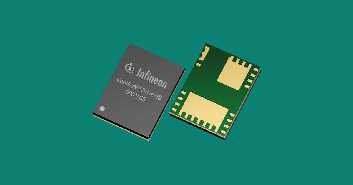
Reducing Layout and Parasitic Challenges in High-Speed Designs
Fast GaN devices punish any unnecessary inductance, and a half-bridge tends to amplify those parasitics when the drivers, bootstrap components, and switches are spread across the PCB. By integrating the bootstrap diode and driver circuitry, the CoolGaN Drive HB G5 reduces the number of traces that carry high di/dt paths, which means fewer opportunities for ringing or unwanted overshoot. That becomes especially significant in compact motor drives or SMPS topologies where magnetics and heatsinks crowd the board and force compromises in routing. The 6 by 8 millimeter TFLGA-27 package with exposed pads helps pull heat into the copper plane without the usual vertical stack of thermal vias, enabling many systems to avoid a dedicated heatsink entirely.
Simplifying Power Stage Design for High-Frequency Operation
GaN’s efficiency advantage appears most clearly when designers push into higher switching frequencies, but maintaining stable behavior at those speeds requires a driver that reacts quickly without introducing its own losses. The HB G5 devices operate from a single 12 volt supply and accept standard-level PWM inputs, which simplifies controller selection and reduces the number of auxiliary rails needed around the half-bridge. Fast undervoltage lockout recovery helps the device behave cleanly during start-up or transient supply drops, preventing the half-bridge from entering undefined conduction states. These attributes matter on dense boards where the power stage interacts with digital logic, sensors, or control networks that may not share the same ground references or transient response.
Four Device Variants for Different Power and Efficiency Targets
The IGI60L1111B1M, IGI60L1414B1M, IGI60L2727B1M, and IGI60L5050B1M versions give designers a range of current and loss profiles suited to low-power motor drives and switched-mode supplies. While the devices share the same integrated structure, their switching characteristics and conduction behavior allow a design to scale without a major layout or control overhaul. This helps teams experiment with higher power density options or magnetics downsizing without rebuilding the entire half-bridge each time. The more predictable thermal and electrical behavior encourages iteration because the designer can focus on the broader converter architecture rather than chasing edge-case parasitics every time a new GaN stage is evaluated.
Learn more and read the original announcement at www.infineon.com
You may also like