 As the US continues to try and limit China’s technological capabilities, Huawei has recently revealed their plans to achieve 1.4nm chips, something that would negate all US efforts. What challenges does China face in creating smaller transistors, what did Huawei announce, and why could this be the end of US capabilities in limiting Chinese engineers?
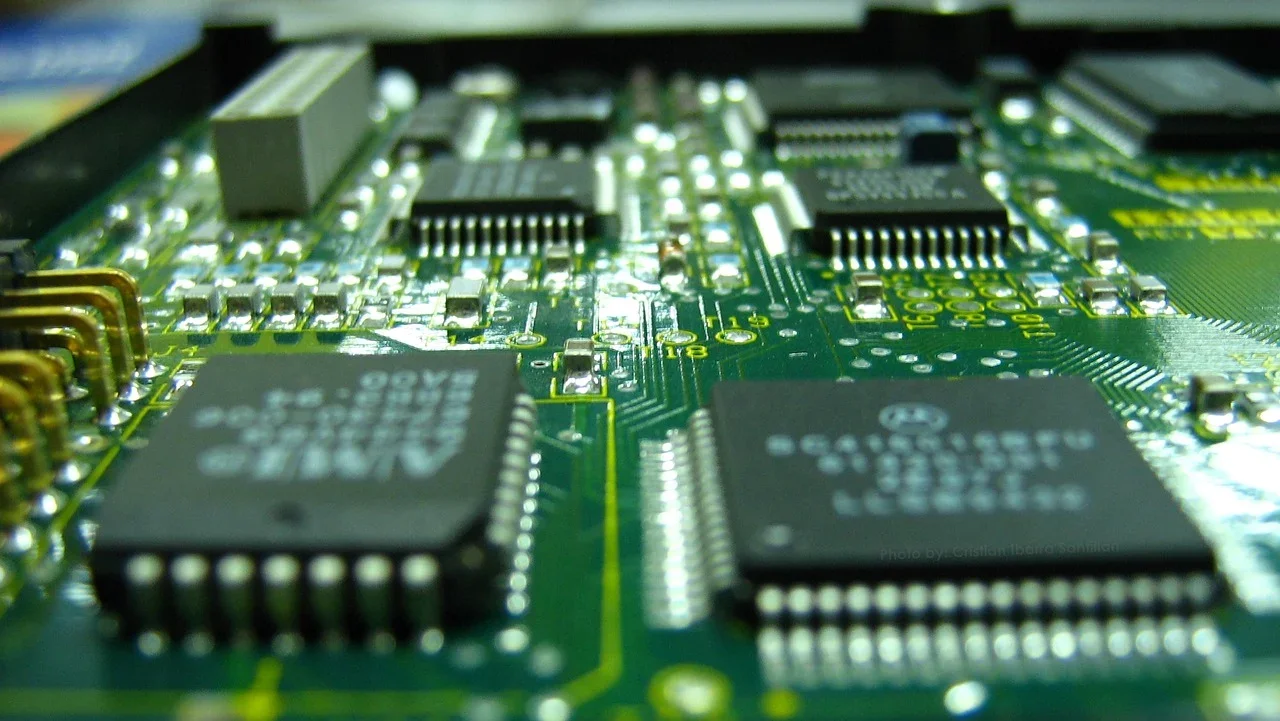
What Challenges Does China Face in Creating Smaller Transistors?
Anyone who has been even remotely involved with electronics over the past two decades will be fully aware of the constant fight between the east and west. While there has always been some level of tension between the two sides, it was when China started to rapidly rise in the economic and technological world stage that saw the US go out of its way to limit Chinese capabilities.
Whether it was limits to the latest technologies, manufacturing services, or even IP, the US has done everything it can to put China at a disadvantage in the semiconductor world, and despite these actions, it appears that China continues to drive its engineers to create their own technologies and solutions.
While China certainly has been able to create semiconductors, they are thus far un able to meet the same capabilities as those developed by the west and nations such as Taiwan. One of the prime reasons for this comes down to the inability for China to access ASML systems that are needed to produce sub 7nm devices, and considering that only one company in the world can make EUV lithographic systems, this gives the US significant power over who can and cannot develop such technology.
This lack of access to advanced lithographic systems has seen China look to more unusual methods for trying to achieve smaller feature sizes, with some reports suggesting that they have even tried to reverse engineer older ASML systems. But, as technology progresses, the ability to shrink transistors becomes increasingly more challenging, and it seems that China is quickly catching up to the west.
Huawei Announces 1.4nm Plans
Recently, Huawei announced a long-term semiconductor roadmap that aims for transistor density equivalent to 1.4nm-class processes by 2031, positioning itself closer to leading global chip manufacturing capabilities. The presentation was made at the Shanghai International Semiconductor Technology Conference, and showed how Huawei is actively looking towards the future, despite the many challenges faced by the US.
However, Huawei’s plan to shrink transistors into the 1.4nm range is not just about physically making smaller transistors, but instead, turning to a new law of transistor scaling. Currently, the law of transistor scaling is based on Moore’s Law, whereby a device that is shrunk in size results in more transistors fitting per unit area, and this allows for more powerful devices.
In the case of Huawei, it is turning to a new law of transistor scaling called τ (Tau) Scaling Law. This law, according to Huawei, is more focused on improving performance and reducing energy consumption, such that signals propagate faster across devices. Thus, instead of focusing on fitting more transistors, focusing on improving signal propagation and energy efficiency can provide a device with equivalent performance.
Furthermore, the new law of transistor scaling, called a new “LogicFolding” architecture, is being used to create a new computational model that improves computation across the entire design space, including the device, the chip, the circuit, and the system.
Finally, Huawei noted that it has already designed and produced 381 chips using the new method over the past six years, demonstrating that it has had time to research and experiment with the new method. It is also expected that LogicFolding-based designs will start to appear in Huawei’s Kirin mobile processors starting in late 2026.
Could this be the End of US Leverage?
When it comes to semiconductors, the US has one critical piece of leverage over all other countries; the ability to restrict who can get advanced tools. As no other company can manufacture EUV systems, and considering that the US has control over who has access to ASML, the US have been able to significantly hold back Chinese developments in the field of semiconductors.
However, if China is able to achieve its goal of developing 1.4nm devices via alternative means, then this could very well be the first time where the US loses its leverage. Even though these devices would be significantly behind those produced by TSMC in terms of node size, if the new technique developed by Huawei provides enough performance boost, then it is possible for China to become self-sufficient in the semiconductor field.
So, if China manages to achieve parity in 1.4nm devices, then has the US lost its leverage?
The answer to this question is no, at least in the short-term, as China would only have achieved parity, but not exceed the capabilities of the US. Furthermore, the US is still responsible for the vast majority of high-performance computing and AI development, meaning that any technological advancement in the West would put China at a serious disadvantage.
Of course, things could change, and it is still possible that China becomes a formidable force for the West to contend with.
You may also like