In a world where reducing transistor sizes is beginning to have less of an effect on device density, researchers are trying to find new ways of packing more transistors on chips. Now, researchers claim to have created a new multi-function transistor that can shrink down designs as much as 75%.
The Challenge with Shrinking Transistors
Ever since the first semiconductors, engineers have been able to improve the capabilities of electronic devices by shrinking transistors. The use of shorter wavelength light, smaller masks, and improved optics allow for transistors to be made physically smaller. Smaller transistors not only allow for more of them to fit onto a semiconductor die, but also resulta in increased performance such as higher operating frequencies and better energy efficiencies.
However, now that we are entering the single nanometre realm, shrinking devices is becoming far more challenging. The need to manage quantum effects in electron behaviour, consider individual atoms in materials, and the challenge of making billions of devices simultaneously all results in increased rates of error, dropping yields, and ever more expensive equipment.
If transistors can’t be shrunk, then how can devices be made to improve?
Researchers Create Multi-Function Transistor For Improved Device Densities
Recognising the challenges faced by modern semiconductors, researchers from the Pohang University of Science and Technology (POSTECH) recently published their work on a new semiconductor device that allows for a single transistor to perform multiple circuit functions simultaneously.
In their paper, published in the American Chemical Society (ACS), the team noted the importance of adding more functionality to chips while keeping transistor counts low. Furthermore, they also highlighted the need for such devices to remain compatible with low-temperature BEOL processes, something which is essential for the latest node technologies.
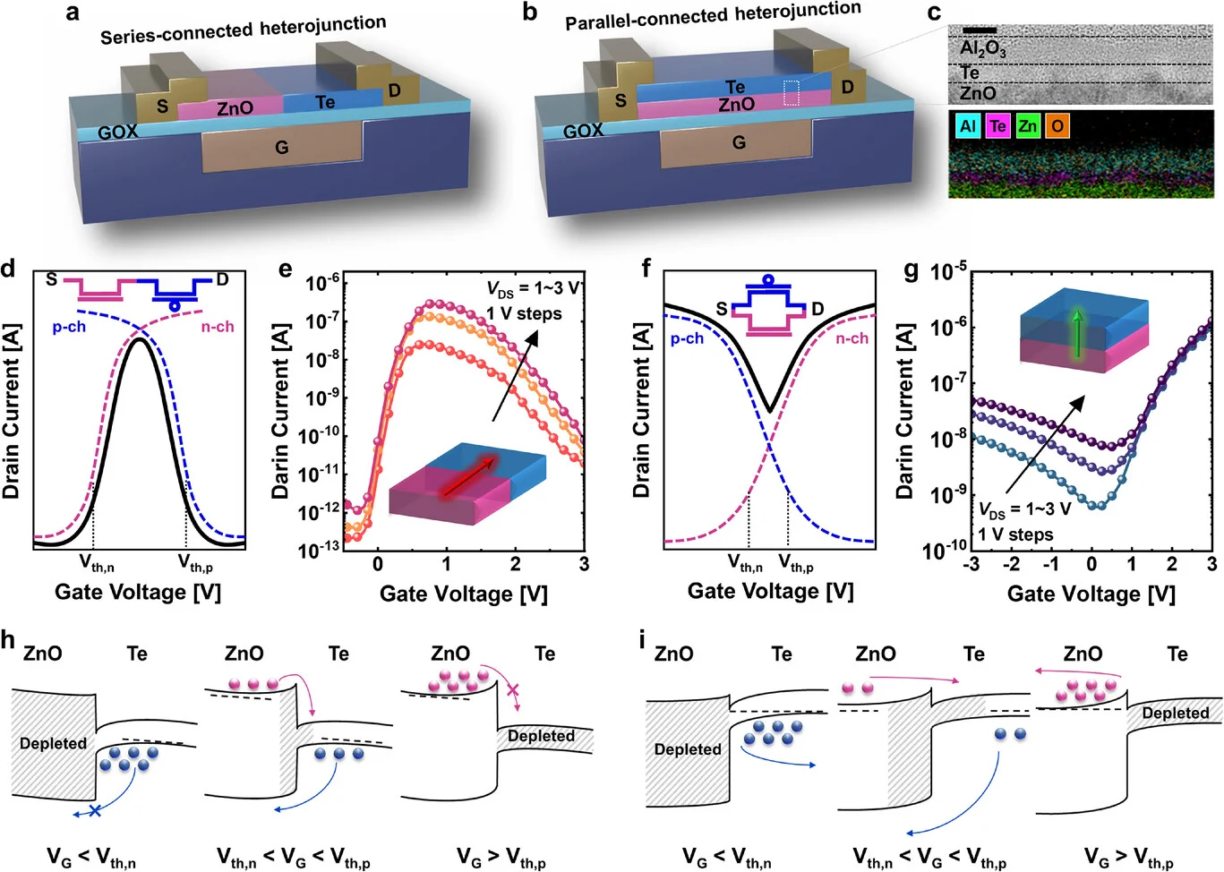
To solve these problems, the researchers created a heterojunction transistor utilising zinc oxide (ZnO) and tellurium (Te). Both of these materials can be deposited as uniform thin films on a silicon substrate, and the resulting semiconductor structure can operate at temperatures lower than 200˚C. This temperature range allows for the device to be integrated into future 3D and highly integrated semiconductor designs.
The resulting device exhibits negative differential transconductance (NDT), whereby the current through the device reduces over specific voltage ranges. However, the device also demonstrated double negative differential transconductance (D-NDT), whereby this behaviour occurs twice in the same device.
This ability to have two separate NDT regions in a single device means that one transistor can perform two different functions simultaneously, thus, removing the need for additional transistors. To demonstrate this capability, the researchers turned to a frequency quadrupler circuit, which takes a single input signal and produces four times the frequency of the original signal. Such a circuit typically requires multiple transistors and supporting circuitry, but the researchers were able to reduce this by approximately 75%.
“Building on the advantages of ZnO–Te D-NDT devices, we believe that they can play a crucial role in next-generation integrated circuits, such as those used in artificial intelligence applications, ultra-compact electronic devices, and 3D-integrated semiconductors.” – Professor Mincheol Shin (POSTECH).
Could This Be The Answer To The Future?
There is no doubt that the device developed by the research team is incredibly impressive, and clearly demonstrates its advantages when used in multi-function roles. However, it should be understood that this type of device won’t replace binary CMOS style gates, but instead, may be more suited for multi-level logic.
In these cases, instead of having two possible logic combinations (a logical 0 and 1), three, four, or more logic combinations can be defined using different voltages, currents, or even conductive states. This allows for a device to represent more information, and thus, have less transistors to perform the same function, thereby increasing transistor density.
However, this also means that these devices are more susceptible to noise, and therefore have stricter margins. Furthermore, the demonstrated device is still in the lab, and we are very far away from having practical devices based on this technology. But, that isn’t to say that with proper funding and time, this could become one of the key technologies of the next generation of devices.
You may also like