
Can a Transistor Be Built from a Single 2D Crystal?
Researchers convert selected WSe₂ layers into WOₓ dielectric, WTe₂ contacts and other electronic regions, creating 2D transistors with a 61.3 mV/dec subthreshold swing and complementary logic.
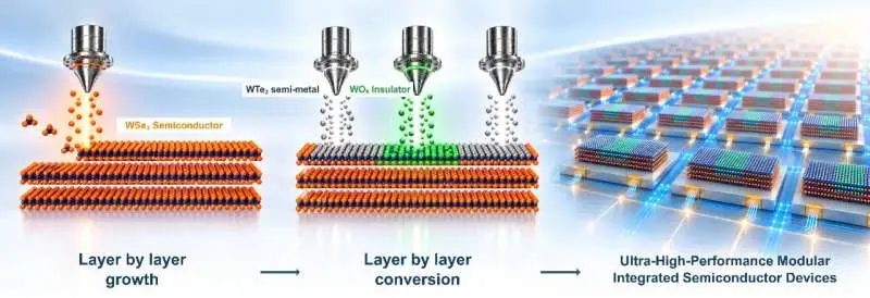
Researchers have built a working transistor by selectively converting different parts of the same layered crystal into the semiconductor, gate dielectric and contact materials needed for the device.
The work, led by the Institute for Basic Science in South Korea, starts with multilayer tungsten diselenide, or WSe₂. Rather than depositing a dielectric on top of the semiconductor and then adding separate metal contacts, the team changes the chemistry of selected regions of the original material. Parts of the WSe₂ become insulating WOₓ, others can be converted into semimetallic WTe₂ or n-type WS₂, while untouched areas remain as WSe₂. scienceview.org
That might sound like an unusual way to build a transistor, but it addresses one of the more stubborn problems facing 2D electronics. Making an atomically thin semiconductor channel is only part of the job. Engineers still need to place a gate dielectric next to it and make low-resistance electrical contacts without damaging the material or creating poor interfaces. At that scale, the parts surrounding the channel can become just as important as the channel itself.
The problem is no longer just making the channel thinner
Two-dimensional semiconductors such as WSe₂ and MoS₂ have attracted interest because they can remain electrically useful even when the active material is only a few atomic layers thick. Conventional silicon channels become increasingly difficult to control as their dimensions shrink, while layered materials offer much stronger electrostatic confinement in the vertical direction.
But those advantages do not automatically carry through to a finished transistor. A gate dielectric has to sit close enough to the channel to control it effectively, yet depositing conventional oxides uniformly onto a van der Waals surface is difficult because the surface has relatively few chemically active bonding sites. Metal contacts create another problem, since deposition can disturb the thin semiconductor and introduce barriers that make it harder to inject charge.
Researchers have tried to work around those issues by mechanically stacking separately prepared 2D materials, creating interfaces held together by van der Waals forces rather than conventional chemical bonds. That can produce exceptionally clean structures in the laboratory, but it is a complicated route if the aim is eventually to make large numbers of devices with repeatable dimensions.
The IBS approach changes the problem. Instead of finding separate materials and then figuring out how to join them together, the team starts with WSe₂ and changes selected layers after the crystal has already been formed. The Science paper describes this as layer-by-layer vapor-phase chalcogen substitution, producing different electronic phases both vertically through the stack and laterally across it. scienceview.org
Converting one crystal into several electronic materials
The process begins by oxidizing selected WSe₂ layers to form WOₓ. That oxide is electrically insulating, allowing it to serve as the gate dielectric while the WSe₂ underneath remains the semiconductor channel.
The conversion can then be taken further. Selected regions can be transformed into WS₂, which behaves as an n-type semiconductor, or WTe₂, which is semimetallic and can be used at the contacts. Because the changes are made locally, the researchers can create several electronic functions from material that originally began as the same WSe₂ crystal. scienceview.org
Controlling how deeply those reactions penetrate is critical. Convert too much material and the channel itself disappears; convert too little and the required dielectric or contact structure is not formed. The researchers report control on the scale of individual WSe₂ layers, with each monolayer measuring roughly 0.7 nm. Temperature and gas pressure are used to determine how far the reaction proceeds through the stack.
This is the part of the work that makes the transistor more interesting than simply another demonstration of a 2D material. The researchers are effectively patterning different electronic properties into a layered crystal after growth, rather than building a device by stacking several independently fabricated materials.
A sub-nanometer gate dielectric
The WOₓ conversion was used to create a gate dielectric with an equivalent oxide thickness below 1 nm. The remaining WSe₂ underneath formed the transistor channel, giving the team an extremely thin gate stack without depositing a conventional oxide directly onto the semiconductor.
The resulting WSe₂ MOSFETs achieved a subthreshold swing of 61.3 mV/dec and an on/off current ratio above 10⁷. Subthreshold swing describes how much the gate voltage has to change to alter the drain current by one order of magnitude. At room temperature, a conventional MOSFET has a theoretical thermal limit of about 60 mV/dec, so 61.3 mV/dec puts the device very close to that boundary. scienceview.org
That does not mean the device has solved transistor scaling on its own. Subthreshold swing is only one measure of performance, and laboratory devices can look very different once questions such as variability, reliability and manufacturing yield are introduced. What the result does show is that converting the upper layers into WOₓ has not prevented the remaining WSe₂ from being controlled effectively as a transistor channel.
The contacts tell a similar story. WTe₂ formed through the same conversion process was used as a semimetallic contact to WSe₂, with the researchers reporting a charge-injection barrier around one-third of that measured with directly deposited platinum contacts. That comparison is important because even a very good channel can be compromised if carriers struggle to enter it through the source and drain contacts.
From one transistor to complementary logic
The team also pushed the process beyond an isolated p-type WSe₂ MOSFET. It demonstrated n-type transistor structures and vertically integrated p-type and n-type devices, eventually using them to form a complementary van der Waals inverter. The inverter produced voltage inversion, showing that the material-conversion approach can be applied to a basic logic circuit rather than only to individual devices. scienceview.org
That still leaves a considerable gap between the laboratory and a commercial logic process. The published work demonstrates control over material conversion and device operation, but it does not establish the wafer-scale uniformity, long-term dielectric reliability or manufacturing throughput that would be needed before this kind of process could compete with established semiconductor fabrication.
Even so, the research changes the way the integration problem can be approached. Much of the discussion around 2D electronics has concentrated on finding a semiconductor thin enough to keep scaling. This work suggests that an equally important question may be how many of the other transistor functions can be created from the same layered material system rather than added afterwards.
Related news
Keep up with the components and technology shaping electronics.
Join the club for member features, engineering discussion and easier access to the latest Component Club content.