 Power designers working on servers, industrial SMPS, and PV inverters are constantly trading conduction loss against switching performance. Conventional three-pin MOSFET packages introduce parasitic inductance between the source lead and the gate driver return path, which limits switching speed and causes additional loss during high-frequency transitions. As supply voltages and power densities rise, these parasitics increasingly determine overall converter efficiency.
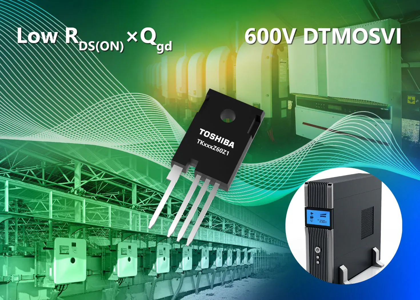
Single-Package Solution for Reduced Switching Loss
Toshiba has expanded its DTMOSVI 600 V family with six new N-channel power MOSFETs that adopt the TO-247-4L(X) package. The design introduces a dedicated source-sense pin that connects directly to the gate driver return, reducing the impact of internal inductance. This allows the actual gate-to-source voltage to follow the driver waveform more precisely, improving switching behaviour and reducing energy lost per cycle.
Key Technical Details
Each device uses Toshiba’s latest DTMOSVI process with an optimised gate structure. The result is a 13% reduction in on-resistance per unit area and roughly a 52% improvement in the key figure of merit, defined as RDS(on) multiplied by Qgd, compared with the previous DTMOSIV-H generation.
For example, the TK024Z60Z1 achieves a typical RDS(on) of 20 milliohms and a gate-drain charge of 37 nanocoulombs, balancing conduction and switching losses for high-efficiency operation. The four-pin TO-247-4L(X) layout also increases creepage distance between the drain and source pins, improving safety margins in high-voltage environments.
Integration and Design Considerations
The new package type differs mechanically from Toshiba’s existing four-pin TO-247-4L outline, so designers should review footprint and clearance dimensions before substitution. The improved source-sense connection enables faster switching transients, especially in hard-switched topologies used in uninterruptible power supplies, photovoltaic inverters and data-centre server PSUs. Circuit analysis can be supported with Toshiba’s G0 and G2 SPICE models, allowing engineers to predict transient behaviour and verify efficiency gains before prototyping.
Why It Matters
These updates reflect how packaging and silicon refinement continue to deliver measurable power savings even at mature voltage nodes. By cutting switching loss without compromising conduction performance, the new DTMOSVI 600 V devices give designers an easier route to meeting efficiency targets in next-generation power conversion systems.
Learn more and read the original announcement on www.toshiba.semicon-storage.com
You may also like