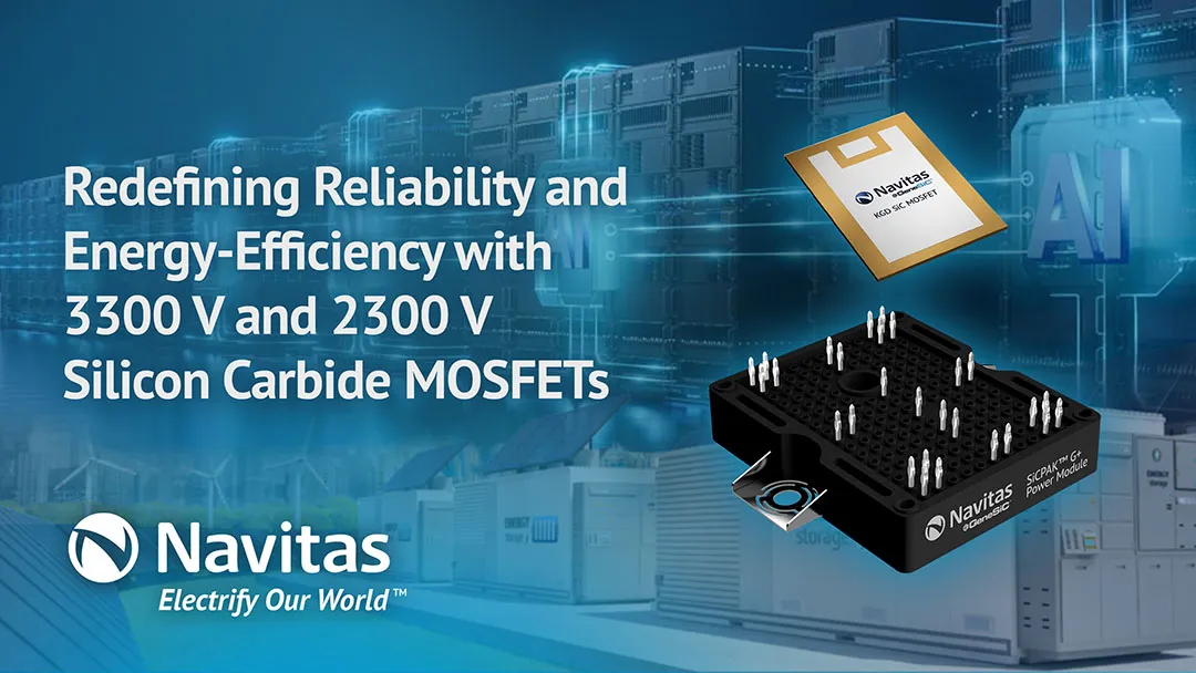
 Engineers working on modern energy infrastructure face a consistent challenge. As power levels grow and switching speeds increase, devices in high voltage stages are pushed harder than ever, often operating near the limits of thermal and electrical stress. Navitas is targeting these environments with a new family of 3300 V and 2300 V silicon carbide devices intended for applications where lifetime, voltage control and predictable behaviour matter more than headline switching numbers. The portfolio spans modules, discrete devices and known good die, giving engineers several paths into ultra high voltage system design.
Electric Field Control At Ultra High Voltage
The platform is built around the company’s Trench Assisted Planar structure. Instead of relying on a single field shaping technique, the TAP approach uses a multi step electric field profile to reduce stress inside the device during high voltage operation. This is an important distinction for engineers designing solid state transformers or multi level converters where long term blocking stability can dictate the overall reliability of the system. Lower stress typically results in better avalanche behaviour, more consistent switching performance at temperature and a wider safe operating region when devices are used in repetitive high energy cycles.
Packaging Designed For Harsh Conditions
For high power modules, the devices appear in the SiCPAK G+ package. The construction is built around an aluminium nitride DBC substrate and uses epoxy resin potting which has demonstrated stronger thermal shock and power cycling performance than silicone gel approaches. This matters in systems that repeatedly cycle between high and low temperatures, such as grid connected inverters, battery storage converters or high duty industrial drives. The design also incorporates high current press fit pins that double the current per pin compared with earlier formats. For designs using discrete parts, the devices are offered in TO 247 and TO 263 7 packages which makes integration into existing layouts more straightforward.
Qualification Beyond Standard Automotive Testing
Navitas has created an extended reliability benchmark referred to as AEC Plus. The idea is to push beyond the standard AEC Q101 and JEDEC requirements by lengthening high temperature and high voltage tests, adding dynamic gate switching conditions and extending temperature and power cycling durations. These tests more closely reflect the conditions seen in utility scale equipment where devices operate for long periods under varying thermal and electrical loads. For engineers, stronger qualification often translates to fewer unknowns when estimating system lifetime or building derating models.
Known Good Die For Custom Module Development
The new devices are also available as known good die for engineers building custom power modules. Each die is tested at room and elevated temperature after dicing and is subject to a full six side optical inspection. The intent is to ensure that only fully screened devices enter higher level assemblies, particularly in multi chip layouts where a single weak die can reduce the reliability of the entire module. For high voltage builds that require tight matching and predictable behaviour, KGD screening can reduce risk and help manufacturers maintain consistent module performance.
Implications For Future High Voltage Designs
The release hints at a longer term push toward 10 kV class devices, which would open the door to even higher density converter stages and more efficient multi level topologies. For now, the 2300 V and 3300 V families give engineers a practical set of tools for the growing demand in data center power distribution, renewable energy conversion and megawatt scale charging. The focus on field control, module robustness and extended qualification standards reflects a steady shift toward power semiconductors that prioritise lifetime and predictable degradation over peak switching metrics.
Learn more and read the original announcement at www.navitassemi.com
You may also like