The Need for Tiny Capacitors in Sensing
Capacitors are one of those components engineers stop consciously thinking about after the first few years of experience. They are everywhere, they are cheap, and they come in every imaginable package. Through-hole, surface-mount, ceramic, tantalum, polymer, you name it, it exists. We drop them into schematics almost reflexively, usually for decoupling, filtering, timing, or energy storage. At the board level, they are so familiar that it is easy to forget how constrained their usefulness actually is once you move outside conventional circuit design.
The limitations of capacitors, however, becomes obvious at scale, or should we say miniature scale. Discrete capacitors, regardless of how small the package is, are fundamentally macroscopic components, even a 0201 ceramic capacitor is enormous when compared to the structures inside modern silicon. This is why memory circuits storing gigabytes of data do not rely on discrete components. Instead, they use integrated capacitors fabricated directly into silicon at the nanoscale.
The same problem appears in high-precision sensing systems, particularly those operating at microscopic or atomic scales. Atomic measurement techniques such as atomic force microscopy rely on MEMS structures that are engineered to oscillate with extreme sensitivity. These systems often use miniature counterlevers that respond to incredibly small forces or surface variations. The signal generated by these movements is frequently capacitive, meaning detection accuracy is directly tied to how much capacitance can be produced between the moving element and its sensor.
From a first principles perspective, the problem looks simple; capacitance increases with plate area and decreases with separation distance. So, in theory, you can just make the lever larger or move it closer to the sensing electrode. In practice, however, both approaches are deeply problematic. Increasing the physical size of the lever increases capacitance, but it also increases mass, and more mass alters the resonant frequency, reduces responsiveness, and can dampen the very oscillations that make the sensor useful in the first place. Larger structures also struggle with spatial resolution, making it harder to probe fine features on a surface.
Reducing the gap between the lever and the sensor is equally attractive, and, equally painful. Smaller gaps dramatically increase capacitance, but they push manufacturing into uncomfortable territory. At microscopic scales, maintaining consistent spacing across a device is extremely difficult, where variations of just a few nanometers can cause performance drift, instability, or outright failure. There is also the risk of stiction, where surfaces adhere due to electrostatic or van der Waals forces, permanently destroying the device.
This is why increasing capacitance in MEMS-based sensing systems is such an active area of research. Engineers and researchers are forced to look beyond simple geometry changes and toward material science, novel structures, and integrated capacitor designs that work at the same scale as the sensor itself. High-permittivity materials, interdigitated structures, and silicon-integrated capacitive elements all exist to extract more signal without compromising mechanical behavior.
In atomic force microscopy and similar applications, signal-to-noise ratio is everything. A stronger capacitive signal means better resolution, lower detection thresholds, and more reliable measurements. Achieving that without breaking oscillation dynamics or manufacturing yield is the real challenge.
Researchers Create World’s Smallest Capacitor
Recently, researchers have demonstrated what is effectively a capacitor pushed to the physical limits of fabrication: a vacuum-gap nano-electromechanical capacitor with plate separations as small as 32 nanometers. At that scale, capacitance is no longer a passive circuit element, but becomes an active participant in mechanical motion, quantum behavior, and fabrication yield management.
The device itself is deceptively simple in concept; a fixed aluminum bottom electrode forms one plate, while a suspended aluminum membrane acts as the other. The gap between them is defined using a sacrificial silicon layer that is later removed via XeF₂ dry etching, leaving behind a precisely controlled vacuum separation. That gap, measured in tens of nanometers, is among the smallest ever reported for a functional, wafer-scale device.
Where things get interesting is how this capacitor is used. Rather than existing in isolation, it forms part of an LC electrical cavity, and in this configuration, the mechanical motion of the suspended membrane directly modulates the cavity’s resonant frequency. Electrical and mechanical resonances become coupled, allowing energy to be exchanged between the two domains.
Shrinking the capacitor gap dramatically increases the parametric coupling rate, and this increases the sensitivity significantly. Small mechanical displacements translate into measurable electrical changes, which is exactly what is needed in applications like ultra-low-noise sensing, quantum electromechanics, and next-generation atomic force microscopy. At these scales, every nanometer matters, and reducing the gap is one of the few levers left to pull.
Fabrication of such devices is where most designs like this fail, and the researchers clearly understood that going in. The device developed by the researchers was built on standard silicon wafers, which immediately improves CMOS compatibility and lowers the barrier to integration. Aluminum was chosen not just for convenience, but for its superconducting properties at cryogenic temperatures. An integrated aluminum nitride piezoelectric actuator allows direct mechanical excitation of the membrane, eliminating the need for external drive mechanisms.
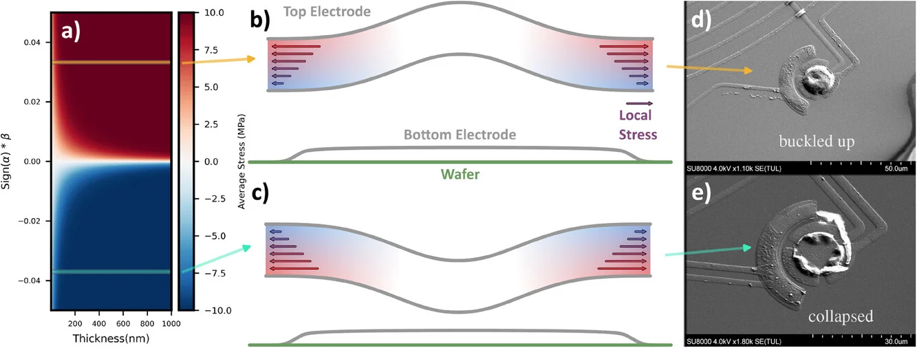
One of the biggest risks with ultra-small gaps is membrane collapse. Electrostatic attraction, residual stress, and fabrication asymmetry can easily cause the suspended plate to pull in and stick. To avoid this, the process ensures simultaneous oxidation on both sides of the top aluminum electrode, balancing stress. A thin silicon capping layer is deposited in vacuum to protect the aluminum surface before release, preventing contamination and oxidation-related failure modes.
Stress control is another factor that turned out to be critical, and the team solved this problem by carefully tuning vertical stress gradients in the aluminum by optimizing sputter deposition power and pressure. Using a low-power, optimized deposition recipe, the researchers achieved wafer-level yields exceeding 90 percent for common membrane sizes.
The devices also behave exactly as intended once fabricated. Electrical measurements confirm proper superconducting cavity operation below aluminum’s superconducting transition temperature, with multiple resonant modes observed. Laser Doppler vibrometry shows that the membranes vibrate freely with high quality factors, indicating low mechanical loss and minimal damping. Interestingly, the capacitor gap shrinks even further at cryogenic temperatures due to thermal contraction mismatch between aluminum and silicon, effectively improving coupling without any additional processing.
Taken together, this platform opens the door to applications that sit well beyond conventional electronics. Quantum electromechanics, ultra-sensitive mass detection, cryogenic AFM, and advanced sensing systems all benefit from strong electromechanical coupling and low noise operation. Sadly, this is not a capacitor you drop onto a PCB, but is instead a precision structure operating at the boundary between mechanics, electronics, and quantum physics, and it shows just how far “tiny” capacitors still have left to go.
Could This Research Be Expanded into Other Areas?
Designing a functional capacitor with a 32 nanometer vacuum gap inside a MEMS structure is undeniably impressive, but it naturally raises a broader question. Is this kind of technology limited to niche scientific instruments, or does it hint at something more general-purpose? As with most breakthroughs at extreme scales, the honest answer sits somewhere in the middle.
A common comparison to make would be dynamic memory. DDR memory relies on capacitors to store charge, and despite decades of scaling, these structures are still physically large relative to modern transistors. In many DRAM processes, storage capacitors remain hundreds of nanometers in at least one dimension, often requiring complex three-dimensional structures just to maintain sufficient capacitance. At this point, the limiting factor in memory density is no longer transistor size, but is the capacitor.
In theory, shrinking capacitors further would allow higher memory densities without radically changing the rest of the memory cell, and from that perspective, research demonstrating stable, ultra-small capacitance gaps is immediately interesting. It reinforces the idea that capacitance can still be extracted at scales smaller than what is currently deployed in commercial memory technologies. Even a modest reduction in effective capacitor size would have a direct impact on memory density, power consumption, and cost per bit.
That said, it is important to also be realistic. The capacitor demonstrated in this research is fundamentally incompatible with DDR memory as it exists today. DRAM capacitors must be densely packed, electrically isolated, extremely uniform, and manufacturable at enormous volumes with near-perfect yield. A suspended aluminum membrane with a vacuum gap defined by sacrificial layers is not something you can drop into a modern DRAM process flow. Even if it were physically possible, the mechanical degrees of freedom alone would be a reliability nightmare in a consumer memory device.
Where the value lies in this research, however, is not in direct reuse, but in transferred understanding. Techniques for defining and controlling ultra-small gaps, managing stress in thin films, preventing collapse, and maintaining high yield at wafer scale are broadly applicable problems. Memory engineers, sensor designers, and materials researchers all run into the same physical constraints, even if the end devices look very different. Concepts developed here could influence future memory architectures that move beyond conventional DRAM, particularly those exploring hybrid electronic-mechanical or charge-based storage mechanisms.
There is also a more general lesson about integration, as this work demonstrates that extreme nanoscale structures can still be fabricated on standard silicon wafers with CMOS-compatible processes. That alone matters significantly, as many promising device concepts die due to the fact they often require exotic substrates or processes that do not scale. Showing that something this delicate can coexist with conventional silicon manufacturing lowers the psychological barrier for other researchers to attempt similarly aggressive designs.
Of course, none of this means you will be buying nanometer-scale capacitors off a reel any time soon. Discrete components live in a very different world, governed by packaging, handling, and mechanical robustness.
You may also like