 AI data center racks and grid converters are not failing because silicon carbide is too slow. They are failing because margins are thinning. Switching frequency keeps rising, bus voltages stay high, thermal envelopes do not grow, and parasitic behavior shows up where it used to hide. At 1200V, small changes in charge and resistance ripple through the entire power stage. Navitas’ 5th generation GeneSiC Trench-Assisted Planar platform is aimed squarely at that pressure point, adjusting device architecture rather than just tweaking die shrink geometry.
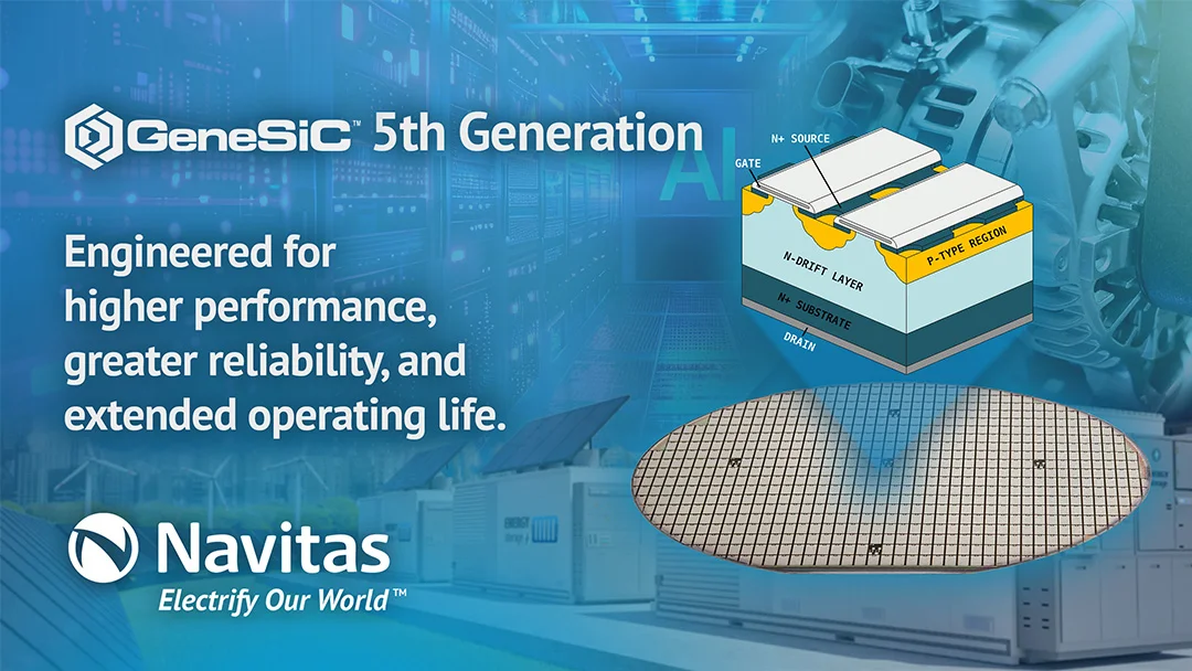
Trench-Assisted Planar Architecture In 1200V Class Devices
The latest GeneSiC platform uses a trench-assisted planar structure that blends the rugged gate characteristics of planar SiC with performance gains from a trench feature in the source region. The architectural shift shows up most clearly in the RDS(on) multiplied by QGD figure of merit, which improves by roughly 35% compared to the prior 1200V generation. That metric matters because it reflects the real switching penalty seen in hard-switched topologies, not just static conduction loss. Lowering that combined figure allows higher switching frequency or reduced thermal burden without redesigning the entire power stage around it.
There is also a shift in how gate charge behaves. An improvement of around 25% in the QGD to QGS ratio tightens control over Miller charge behavior. When paired with a stable threshold voltage at or above 3V, the device becomes less susceptible to parasitic turn-on in noisy layouts. Anyone who has chased a false turn-on event during double pulse testing understands how quickly that can derail a design.
Soft Body Diode Behavior And Dynamic Performance
Dynamic losses in SiC are not only about turn-on and turn-off edges. Reverse recovery behavior and output capacitance shape real world efficiency as much as on resistance. The 5th generation platform adjusts the RDS(on) multiplied by EOSS characteristic to reduce stored energy in the output capacitance, while integrating what Navitas describes as a soft body diode structure. In practice, softer commutation reduces abrupt current transitions and helps limit electromagnetic interference during high-speed switching. That shows up on the scope long before it shows up in a datasheet table.
For engineers pushing fast edges in server power shelves or industrial drives, these subtle waveform differences can determine whether additional filtering is required. You only notice it after probing a half-bridge at full load and seeing less ringing than expected.
Reliability Under Real Switching Stress
The platform also targets reliability under aggressive operating conditions. Extended high temperature reverse bias and gate bias testing durations have been increased, along with dynamic reverse bias and dynamic gate switching stress profiles intended to mirror real switching environments. Threshold voltage stability over prolonged switching stress is emphasized, alongside gate oxide lifetime projections at elevated gate voltages and temperatures.
There is also attention paid to cosmic ray resilience, reflected in low failure in time rates for high altitude and high uptime applications. That becomes relevant in data centers and grid infrastructure where uninterrupted operation is assumed rather than requested. Reliability is not an abstract metric when racks are expected to run continuously for years.
Positioning 1200V SiC In AI And Grid Power Stages
Navitas’ 4th generation GeneSiC platform already addressed ultra high voltage segments at 2300V and 3300V. This 5th generation shift focuses on the 1200V class where most AI server power shelves, industrial drives, and renewable converters operate. Bandwidth alone does not define performance at these levels. Switching loss, gate stability, output capacitance behavior, and long term robustness all converge in the same few square millimeters of silicon carbide.
The incremental improvements in figure of merit and dynamic stability may look modest in isolation. In dense power stages operating near thermal limits, they change how aggressively designers can push frequency and shrink magnetics. That pressure is not going away.
Learn more and read the original announcement at www.navitassemi.com
You may also like