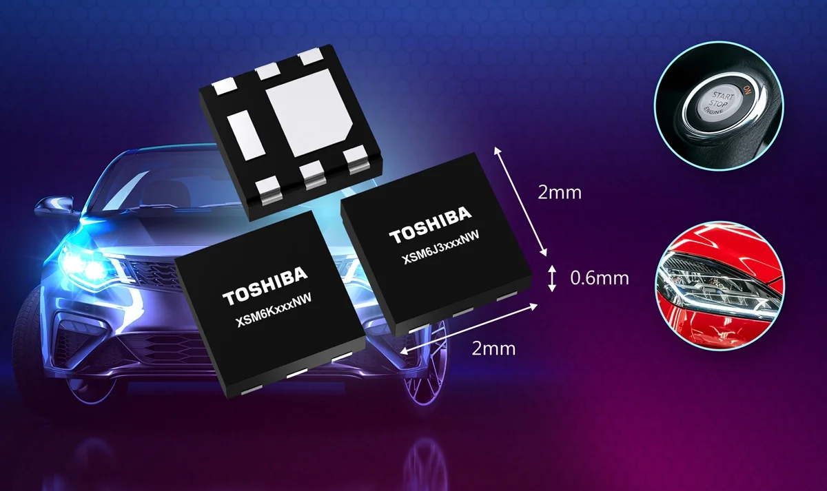
 Automotive MOSFET development is no longer just a story about lower resistance or higher current in familiar footprints. More of the differentiation is starting to show up in packaging, inspection compatibility, and how well a device fits modern assembly flows. Toshiba’s latest release makes that shift fairly obvious, with five new automotive MOSFETs housed in its DFN2020B(WF) package with wettable flanks.
The lineup includes four N-channel devices, XSM6K361NW, XSM6K519NW, XSM6K376NW, and XSM6K336NW, along with the P-channel XSM6J372NW. These are automotive MOSFETs used for switching and power-control functions in systems such as ECU DC-DC converters and LED headlamp load switches, where package size, mounting quality, and inspection access can matter just as much as the transistor itself. In a typical vehicle power board, that small switching device may sit in a crowded section surrounded by controllers, passives, connectors, and thermal constraints that do not leave much room for compromise.
The Package Matters More Than The Press Release Suggests
It is easy to read a MOSFET announcement and go straight to the silicon, but this release is really about package behavior. Toshiba is putting the DFN2020B(WF) front and center because the wettable flank structure improves solder wettability while also making the solder fillet easier to inspect with automated optical inspection equipment. That second point is not a cosmetic improvement. On dense automotive boards, visible solder joints are one of those details that only seem boring until inspection becomes uncertain.
The company also says the new package shows around 23% greater solder-joint mounting shear strength than its existing SOT-23F package. That is the sort of comparison that feels more meaningful in automotive than in ordinary low-voltage switching applications. Long service life, vibration exposure, and thermal cycling all make package integrity part of the device story whether designers want it to be or not.
Smaller Outlines Usually Bring New Tradeoffs
The DFN2020B(WF) package comes in at a typical 2.0 mm by 2.0 mm by 0.6 mm, which puts it well below the size of Toshiba’s SOT-23F package at 2.4 mm by 2.9 mm by 0.8 mm. According to Toshiba, that cuts mounting area by around 43% and lowers package height by roughly 25%. Those are not trivial reductions in modern vehicle electronics, where a few saved millimeters can make routing, placement, and enclosure constraints noticeably easier.
What makes the release more credible is that the smaller footprint is not being presented as a pure density play with hidden penalties left for later. Toshiba highlights the XSM6K361NW with a maximum power dissipation rating of 1.84 W, compared with 1.2 W for its existing SSM3K361R in SOT-23F. That does not automatically settle every thermal question, but it does show the company is trying to avoid the usual trade where miniaturization arrives first and real power handling quietly falls behind it.
Why AOI Visibility Has Become A Real Design Consideration
Automotive packaging has been moving in a direction where manufacturing visibility now influences device selection much more directly. Wettable flanks help because they give inspection systems a clearer view of the solder condition at the edge of the package, which becomes increasingly useful as outlines shrink and assemblies become more crowded. In practice, that makes the package part of the production strategy instead of just the enclosure around the die.
This is one of the reasons the launch feels more interesting as a packaging development than as a conventional transistor update. The silicon still matters, obviously, but the stronger angle here is that Toshiba is trying to make smaller automotive MOSFETs easier to mount, easier to inspect, and harder to dislodge once assembled.
A Broader Move In Automotive Power Packaging
Toshiba also notes that all five new devices comply with AEC-Q101, and that PPAP support under IATF16949 is available. That places the parts where they need to be for serious vehicle programs, but the longer-term signal is probably in the company’s roadmap. Toshiba says it plans to expand the MOSFET lineup using DFN2020B(WF) and to introduce future 2-in-1 automotive MOSFET products in DFN2020(WF).
That suggests the package itself is becoming a platform direction. In automotive power electronics, that makes sense. Once designers start asking for smaller devices without giving up inspectability or mounting robustness, the package stops being a background decision and starts becoming one of the more useful differentiators on the board.
Learn more and read the original announcement at www.toshiba.com
Technology Overview
Toshiba has introduced five automotive MOSFETs in its DFN2020B(WF) package with a wettable flank structure. The package measures 2.0 mm × 2.0 mm × 0.6 mm and is designed to improve solder wettability, solder fillet visibility for automated optical inspection, and solder-joint mounting strength in compact automotive power applications. The devices comply with AEC-Q101, and PPAP support under IATF16949 is available.
Frequently Asked Questions
What are Toshiba’s new DFN2020B(WF) MOSFETs used for?
They are used for compact automotive switching and power-control applications such as DC-DC converters for ECUs and load switches for LED headlamps.
What is the size of Toshiba’s DFN2020B(WF) package?
The DFN2020B(WF) package has a typical size of 2.0 mm × 2.0 mm × 0.6 mm.
You may also like