 As engineers continue efforts to reduce the size of transistors, some are concerned that we are now hitting hard physical limits. But recent calculations and simulations have shown that sub 2nm devices are more than possible, opening up new opportunities for devices to continue getting smaller.
What Challenges do Sub 2nm Devices Face?
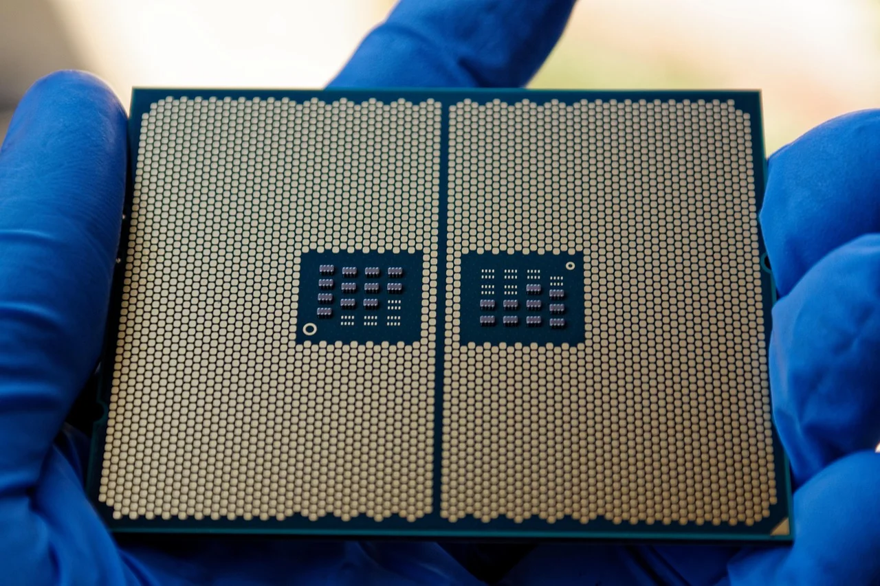
Since the first integrated circuits, making transistors smaller has been the prime factor in improving semiconductor technologies. By making transistors smaller, more transistors can fit on a given die, resulting in increased logic densities, memory capacities, and accelerator capabilities.
But making transistors smaller also reduces their energy consumption per transistor, while also allowing for higher frequency operation. In fact, it is this reduction in energy consumption that has resulted in mobile devices becoming increasingly powerful, with devices no longer needing to rely on energy conserving modes to try and increase their battery life.
However, now that transistors are approaching the size of less than 4nm, we are faced with a whole new set of challenges that go well beyond what was seen at the 200nm node. For example, quantum effects have always been a problem, but when gates and channels are less than a few nm, these effects become even more problematic, almost impossible to mitigate against.
Then there is the issue with EUV and lithography light, as feature sizes are now far smaller than the wavelength of light being used to make them. As such, extremely specialized masks are needed, taking advantage of diffraction to create structures. However, the machines needed to create these masks are extremely expensive, and only one company in existence controls their manufacture, giving them a monopoly on EUV lithography equipment.
Finally, even if a 5nm device is possible, wafer purity, yields, and customer demand will all present massive hurdles that may see such devices in short supply.
Researchers Did the Math and Discovered Sub 2nm Is Possible!
Recently, researchers at the KAIST (Korea Advanced Institute of Science & Technology) have developed an advanced atom-level simulation method to determine how small future transistors can become before quantum effects begin to degrade their performance.
One of the biggest problems currently faced by the semiconductor industry is quantum tunneling, whereby electrons can effectively “teleport” through barriers from one side of a barrier to the other. This is particularly troublesome for transistors as it makes it harder to control the flow of current through a channel. The use of thicker barriers can help prevent this, but this comes at the cost of increasing contact resistances, thereby reducing transistor performance.
To overcome this challenge, the team first had to develop a simulation method capable of directly observing individual atoms and their interactions. This was achieved with the development of their MS-DFT (Multi-Space Constrained-Search Density Functional Theory), which allows for accurate quantum mechanical simulations of real materials.
However, once the basic operation of the transistor was determined, the team then performed a series of “virtual experiments” to explore contact resistance and electron transport on the atomic scale. This was achieved with the use of the virtual transfer length method (TLM), which has previously been used to study bulk semiconductors.
The researchers then applied their method to a monolayer molybdenum disulfide (MoS₂), which is a 2D semiconductor that has garnered significant attention as a potential future channel material. The results of their simulation showed that the critical tunneling length depended on the material choice, with the electron leakage depending on the work function of the metal contact and the contact geometry. Overall, the researchers were able to demonstrate that electron leakage could be controlled in several material combinations, with dimensions expected to fall below the 4nm mark.
Just How Far Can We Shrink Transistors?
It turns out that transistor action has already been demonstrated on individual atomic scale devices, but the question isn’t whether a transistor can be made smaller, but if those devices can be made reliably small enough to produce functional devices.
Because when it comes to semiconductor devices, it’s not just about making a single transistor small, it’s about making 1 billion of them at the same time and getting them to work correctly at absurd operating speeds.
Even though the researchers demonstrated that 2nm is well within the realm of possibility, it doesn’t mean that we will see such devices anytime soon.
So, while it is possible that sub 2nm could definitely happen, it is also likely that going forward, we will see a gradual slowdown in transistor shrinkage, with the next generation of devices exploring alternative concepts, such as stacked dies, stacked transistors, and 3D devices.
You may also like