The Journey Beyond 2nm Devices
While we are still a few years away from having 1nm devices, we are at a point in time that is truly exciting; we are about to enter the realm of 1nm. Now, when engineers get to this point, quantum effects and atomic-scale variability make device behavior non-intuitive. To try and get transistors to work at such scales is a task that is almost impossible to achieve.
Of course, with enough money and engineering effort, much becomes possible, and this is certainly true when it comes to semiconductor manufacturing. At these scales, the need for extremely expensive EUV machines becomes paramount (such as ASML's latest high-NA EUV systems, which are expected to cost nearly $400 million). At the same time, materials need to be of such purity that impurities must be controlled at the atomic scale.
But the problem with this is that the cost sensitivity of such devices is so great that a single batch of devices with a failure rate above some arbitrary value could see major economic issues. Making matters worse, the cost to build such facilities also skyrockets, and the time taken to build them increases.
This means facilities can take years to build and ramp to volume; by the time they are fully operational, process nodes and recipes at other foundries may have advanced, and settings are not directly transferable. In fact, this is one of the biggest challenges faced with modern semiconductor manufacturing; each facility has to do its own thing and calibrate its equipment to produce devices.
Thus it is no longer enough to simply purchase the same equipment as another foundry and use the same process recipes and calibrations. This, is why engineers continue to struggle with reducing node sizes.
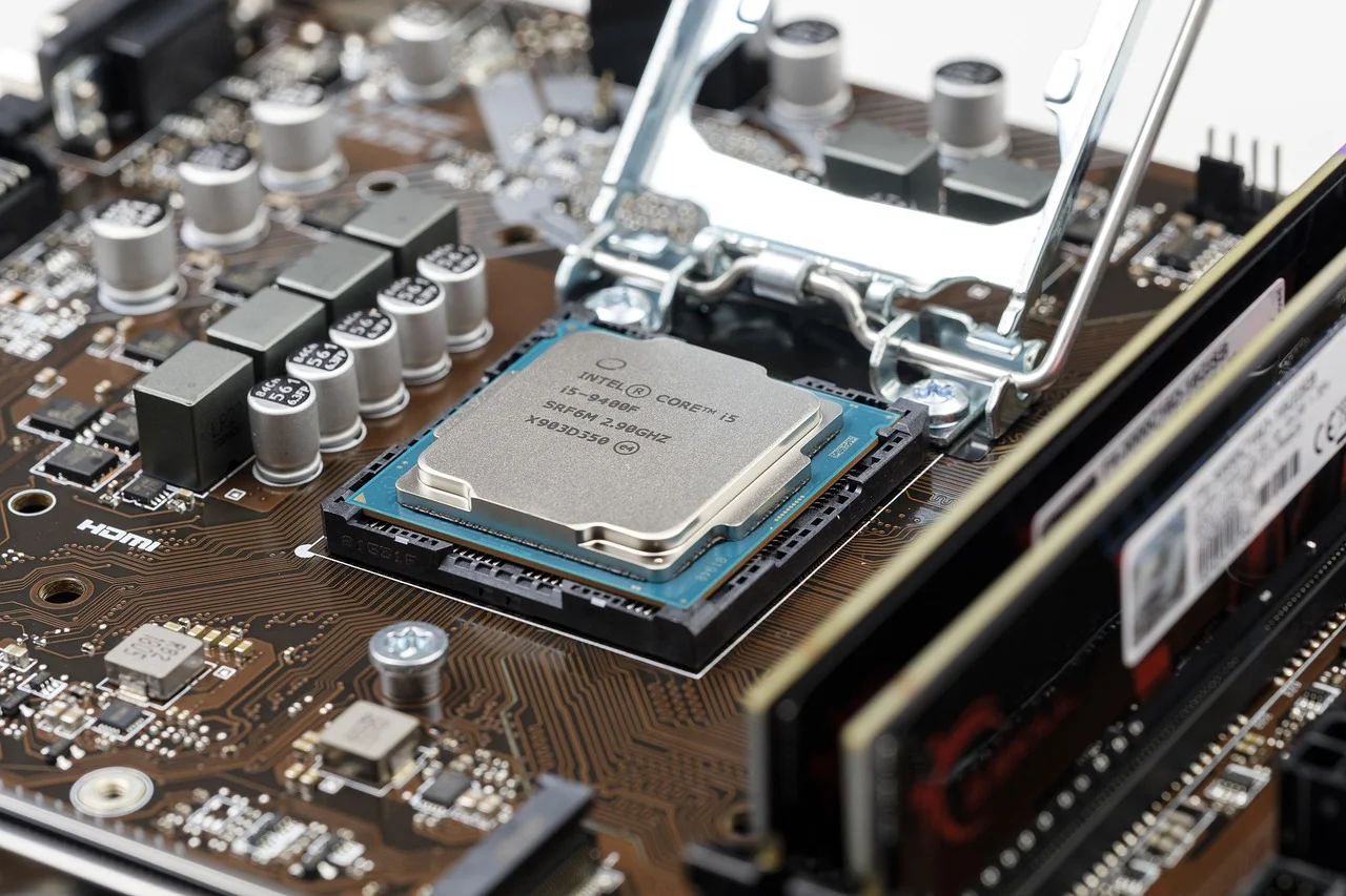
Intel Breaches the 2nm Boundary with its 18A Panther Lake Architecture
Recently, Intel announced plans to launch its latest chip, Panther Lake, at the Consumer Electronics Show which will be fabricated using the company's 18A process technology. This launch of the Panther Lake architecture is seen as a key step for Intel to regain its position in semiconductor manufacturing, and also help Intel expand its foundry services into the US for the first time.
While the announcement of Panther Lake was made, there was also mention of how there was discussion of U.S. government support for semiconductor manufacturing (via the CHIPS Act). However, what was of more interest to us here at The Component Club is how Pat Gelsinger has placed great emphasis on Intel becoming a foundry service provider.
As we have mentioned numerous times, the semiconductor industry is in a state of crisis due to the numerous challenges faced by Taiwan and China, and the West's dependency on these countries for advanced semiconductors. To try and combat these challenges, the US (and other nations) have launched various CHIPS act which provides subsidies and tax breaks to those in the semiconductor industry who invest in new foundries.
But while many companies have taken advantage of the CHIPS act, Intel has been criticized for not expanding its foundry capacity as aggressively as some competitors. Thus, the introduction of Panther Lake, which is expected to be manufactured in the US, could see Intel once again become a major player in the US foundry market.
With the potential to manufacture cutting-edge semiconductors, many major chip designers including AMD, NVIDIA, Qualcomm, and Apple may even look towards Intel for such services. However, Pat Gelsinger also noted that restoring advanced semiconductor manufacturing from Asia back to the US won’t happen overnight, and could take many years before the US is able to compete.
The move toward Intel's 18A (an angstrom-class node roughly in the sub-2nm/1.8nm neighborhood) highlights why the industry is increasingly focused on the extreme challenges of angstrom/sub-2nm manufacturing. At these scales, physics behaves differently, equipment costs (for example, ASML's upcoming high-NA EUV systems are widely reported to cost nearly $400 million each) and material purity requirements become extreme. Fabs and their calibrations are site-specific and take years to bring online, and a single failed batch can have huge economic consequences. This makes manufacturing at sub-2nm densities highly scientific, tightly controlled, and very expensive.
What does the future hold for semiconductors going beyond 1nm?
This is not the end of semiconductor technology, and it will continue to develop. We are approaching the 1nm realm, where quantum effects and other nanoscale physics begin to dominate device behavior.
However, we may start to see a significant slowdown in the shrinking of semiconductor technology. Even though researchers have already made transistors on the atomic scale, that doesn’t mean that they will ever be suitable for production.
Manufacturing at these scales requires extremely precise tools (ASML's most advanced EUV/high-NA systems cost on the order of hundreds of millions of dollars), and material purities and process control become extremely demanding. Fabs capable of producing at such densities typically cost billions to build, can take years to construct and qualify, and when they come online the process settings must be tuned and calibrated for that specific site rather than simply imported from another facility.
Furthermore, there are diminishing returns on making transistors smaller, and eventually manufacturers will need to start using clever tricks to increase the number of transistors on a design without reducing the size of transistors. For example, chiplets can increase effective transistor count by combining multiple dies (tiling) or by 3D packaging/stacking (the latter is what Intel’s Foveros implements).
Another example would be wafer-scale integration, where a single device is made physically much larger (for example, some AI accelerator vendors pursue wafer-scale chips). Of course, multi-layer active devices could come about, but this is an extremely hard task to achieve. Multiple companies are pursuing 2nm-class and 'angstrom'-class technologies (TSMC, Samsung, and Intel among them), and the future of electronics has never been more exciting. This makes manufacturing below ~2nm an intensely scientific, tightly controlled, and expensive endeavor.
You may also like