
 ©ASML
©ASML
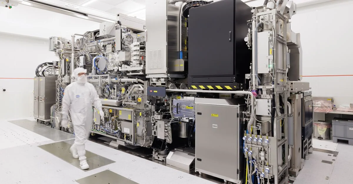
High-NA EUV has spent the past few years looking like a technology belonging to the semiconductor industry's future. The machines are enormous, extraordinarily complex and expensive, while much of the discussion around them has focused on the manufacturing challenges that will emerge as chipmakers attempt to push lithography beyond today's EUV systems.
Intel Foundry's latest numbers suggest that future is starting to arrive.
The company says more than one million wafers have now been processed using High-NA EUV across tool certification, research and development and volume production. More importantly, selected layers of Intel Core Ultra Series 3 processors, code-named Panther Lake, are already being manufactured using the technology.
That doesn't mean conventional EUV is about to disappear. Far from it. But on the same day, Samsung announced plans to introduce High-NA EUV into DRAM high-volume manufacturing in 2028, while TSMC said it intends to use the technology for advanced-node high-volume manufacturing from 2030.
High-NA EUV is no longer simply about proving that a new lithography system works. The industry is starting to work out how to use it at scale.
What Actually Changes With High-NA EUV?
Modern semiconductor manufacturing depends on lithography to transfer increasingly small patterns onto silicon wafers. EUV systems use light with a wavelength of 13.5 nm to pattern features considerably smaller than those possible with earlier deep ultraviolet lithography. But wavelength is only part of the equation. The numerical aperture of the optical system also affects the resolution that can be achieved.
ASML's existing NXE EUV systems use optics with a numerical aperture of 0.33. Its newer EXE High-NA platform increases this to 0.55, allowing smaller features to be resolved on the wafer.
That matters because chipmakers have increasingly relied on multiple patterning steps to create features beyond what a single exposure can resolve. Each additional patterning step adds process complexity, time and opportunities for variation. Improving the resolution of the lithography system can potentially allow some of those structures to be patterned more directly.
The attraction is fairly obvious. The difficulty is doing it reliably enough, quickly enough and economically enough to manufacture millions of chips.
Intel Is Already Using It
Intel received the first commercial High-NA EUV system from ASML in 2024. Two years later, the company says High-NA is being used in high-volume manufacturing on selected Panther Lake layers.
The million-wafer figure needs some context. Intel says that total includes wafers processed during early tool certification and testing, research and development, and volume production. It doesn't mean one million production wafers have been manufactured entirely using High-NA EUV. Even so, it represents a considerable amount of operating experience with a technology that only recently moved out of the development stage.
Intel also says overlay, throughput and system availability are meeting its expectations. On its Intel 18A process, layers produced using High-NA are delivering performance that meets or exceeds comparable layers patterned using ASML's existing 0.33 NA NXE platform.
That is perhaps more important than the raw wafer number. A lithography system can demonstrate impressive resolution in development, but semiconductor manufacturing depends on considerably more than resolving the smallest possible feature. Patterns need to align accurately with previous layers, wafers need to move through the equipment at a useful rate and the machine needs to remain available often enough to justify putting it into a production line.
High-NA now appears to be moving into that part of its development.
Samsung Wants to Take High-NA Into DRAM
Logic processors aren't the only place this technology could appear.
Samsung says it plans to introduce ASML's High-NA EUV technology into high-volume DRAM manufacturing by 2028, which the companies describe as the first planned industry adoption of High-NA for DRAM production.
Memory presents its own scaling challenges. Increasing DRAM density requires manufacturers to continue shrinking structures while maintaining the electrical characteristics needed to store and access data reliably. As those structures become smaller, lithography becomes one of the constraints on how far existing manufacturing processes can be pushed.
Samsung expects the additional resolution provided by High-NA to extend the DRAM scaling roadmap while potentially simplifying some process steps.
The timing is interesting. If Samsung reaches high-volume DRAM manufacturing with High-NA in 2028, the technology will have moved from early logic production into one of the world's highest-volume semiconductor markets within only a few years.
TSMC is taking a slightly longer view. The foundry says it intends to introduce High-NA into high-volume manufacturing for advanced nodes beginning in 2030, with the number of layers requiring the technology expected to increase as transistor architectures become more complex.
Taken together, the three announcements show different stages of the same transition. Intel is already using High-NA on selected production layers. Samsung is preparing to use it for memory. TSMC expects its use to expand as future logic processes become harder to manufacture with existing lithography.
Better Resolution Creates a Different Problem
Increasing the numerical aperture comes with a trade-off. ASML's High-NA system exposes a smaller field than its conventional EUV equipment.
That creates a problem for chips or layouts that don't fit within the available exposure area.
One solution is stitching. Instead of exposing the entire pattern as a single field, separate exposures can be accurately joined together on the wafer. Intel is already developing this approach and says customers can use High-NA with today's standard 6-inch photomasks either by designing within the available field or using its stitching capabilities and process design kit.
Stitching isn't simply a matter of putting two pictures next to one another. The adjoining exposures need to align with sufficient precision that the resulting structure behaves as though it were patterned continuously.
The fact that Intel and ASML are now presenting work specifically around stitching for manufacturing shows how the High-NA discussion is changing. The question is becoming less about whether the optics can achieve the required resolution and more about how the surrounding manufacturing process adapts to them.
And that leads to another change that could be coming to semiconductor fabs.
Why Does High-NA Need a Bigger Photomask?
For decades, semiconductor manufacturing has been built around the 6-inch photomask format. High-NA can operate using those masks, and Intel is demonstrating that it can already do so in production.
But the industry is now considering something much larger. TSMC and ASML have launched an initiative to develop a 12-inch photomask platform for High-NA EUV. Samsung has also joined the effort, while Intel says it has been working with ASML and the wider mask ecosystem on larger-format masks for more than three years.
The reason isn't simply to make the mask bigger for the sake of it. A larger mask could reduce some of the field-size constraints associated with High-NA, improve scanner productivity and reduce the need to stitch patterns together. Getting there will take time. TSMC and ASML are targeting a 12-inch mask pilot line by 2031, with full lithography-system readiness for advanced-node production around 2033.
Changing a mask format that has been used across the semiconductor industry for decades also affects far more than the mask itself. Mask makers, inspection equipment, handling systems, materials, automation, EDA tools and lithography equipment all need to work around the new format.
That perhaps explains why the initiative is being discussed more than half a decade before the intended production transition. High-NA may be an ASML lithography technology, but using it at scale depends on an ecosystem considerably larger than ASML.
High-NA Is Becoming an Industry, Not Just a Machine
It is easy to focus on the extraordinary engineering inside an ASML High-NA scanner. Increasing numerical aperture from 0.33 to 0.55 requires a fundamentally different optical system, and the resulting equipment represents one of the most complicated manufacturing tools ever built.
But the announcements from Intel, Samsung and TSMC point towards a different stage in the technology's development.
Intel is now talking about wafer volumes, overlay, throughput and production layers. Samsung is talking about DRAM manufacturing in 2028. TSMC is planning advanced-node production from 2030. Meanwhile, chipmakers, mask suppliers, equipment companies and EDA providers are already discussing how to change a photomask format that has existed for decades.
Those aren't really questions about whether High-NA EUV works. They're questions about how the semiconductor industry builds manufacturing infrastructure around it. Conventional 0.33 NA EUV will continue to manufacture enormous numbers of advanced chips, and High-NA is unlikely to suddenly replace every EUV layer. The more likely transition is gradual, with chipmakers introducing High-NA where its additional resolution justifies the cost and complexity.
Intel's Panther Lake production suggests that process has already started.
The more interesting question now may be what happens as High-NA moves beyond selected layers and early adopters. If Samsung brings it into DRAM in 2028 and TSMC follows with advanced-node production from 2030, the technology could move surprisingly quickly from being an exotic new lithography system to a standard part of leading-edge semiconductor manufacturing.
And if the industry really does move from 6-inch to 12-inch photomasks to accommodate it, High-NA won't simply have changed the scanner. It will have forced a much larger part of the semiconductor manufacturing ecosystem to change with it.
You may also like