
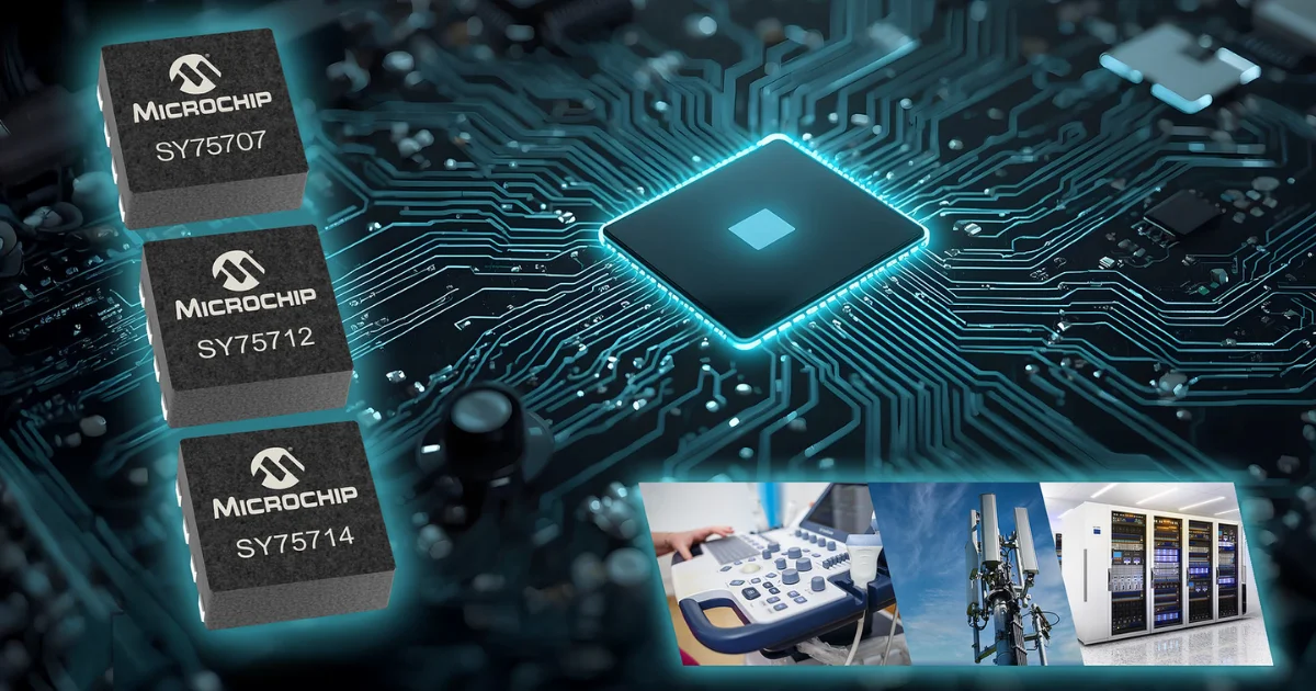
 Microchip has introduced the SY757xx family of low-voltage LVCMOS clock buffers for distributing clock signals between FPGAs, SoCs and other components operating across different voltage domains.
The new devices provide 1.2 V clock outputs while supporting input and supply options extending up to 3.3 V. This allows higher-voltage clock sources and components to interface with newer FPGAs, SoCs, AI accelerators and CPUs that require lower-voltage clock signals.
Microchip has introduced the SY757xx family of low-voltage LVCMOS clock buffers for distributing clock signals between FPGAs, SoCs and other components operating across different voltage domains.
The new devices provide 1.2 V clock outputs while supporting input and supply options extending up to 3.3 V. This allows higher-voltage clock sources and components to interface with newer FPGAs, SoCs, AI accelerators and CPUs that require lower-voltage clock signals.
The family operates across frequencies from 0 Hz to 250 MHz, with additive jitter as low as 26 fs. Three devices are already in volume production, while another eight configurations are currently sampling in limited quantities.
Clock Distribution Across Different Voltage Domains
Lower operating voltages in newer processors are creating an interface problem for boards that also contain components running at higher voltage levels. Microchip developed the SY757xx family to provide clock fanout and voltage translation within a single device rather than using discrete components to reduce the clock signal voltage.
Discrete voltage-divider implementations can introduce duty-cycle distortion and reduce signal integrity margins. The SY757xx buffers translate the clock while maintaining the timing accuracy required by high-speed FPGA, SoC and CPU platforms.
Across the wider family, devices can accept single-ended LVCMOS inputs from 1.2 V to 3.3 V or differential inputs from 1.8 V to 3.3 V, depending on the configuration. Output options cover 1.2 V to 1.8 V LVCMOS, with output-enable fanout versions also available.
This allows the buffers to connect devices operating from different voltage rails without adding separate level-translation circuitry to the clock path.
Three Devices Enter Volume Production
Microchip has initially moved the SY75707TWL-TR, SY75712TWL-TR and SY75714TWL-TR into volume production.
The SY75707TWL-TR accepts a differential input and provides two LVCMOS outputs in an 8-pin VDFN package. The SY75712TWL-TR and SY75714TWL-TR provide two and four LVCMOS outputs respectively and are supplied in 8-pin TDFN packages.
The remaining eight SY757xx devices are sampling in limited volumes and extend the available input, output and fanout configurations.
Microchip is targeting the family at clock distribution in high-performance computing and embedded platforms using FPGAs, SoCs and CPUs. Applications include AI and machine learning acceleration, embedded vision and video processing, industrial control, networking and communications, and signal-processing systems.
The SY75707TWL-TR, SY75712TWL-TR and SY75714TWL-TR are priced from $0.50 to $0.83 per unit depending on configuration in quantities of 10,000.
Learn more and read the original announcement at microchip.com.
Technology Overview
The Microchip SY757xx family consists of low-voltage LVCMOS clock buffers designed to distribute clock signals between components operating across different voltage domains. The devices support 1.2 V clock outputs, frequencies up to 250 MHz and additive jitter as low as 26 fs.
FAQs
What is the Microchip SY757xx family?
The SY757xx family consists of low-voltage LVCMOS clock buffers designed for clock distribution and voltage translation in systems using FPGAs, SoCs, CPUs and other high-performance processors.
What voltage levels do the SY757xx clock buffers support?
Depending on the device, the family supports clock inputs and supply options across the 1.2 V to 3.3 V range, with LVCMOS output options from 1.2 V to 1.8 V.
What is the additive jitter of the SY757xx family?
Microchip specifies additive jitter as low as 26 fs, with the family supporting clock frequencies from 0 Hz to 250 MHz.
You may also like