
Diodes Launches 2 GHz Low-Jitter Clock Buffers for Servers and Network Switches
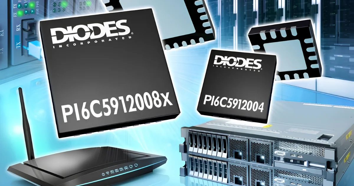 Diodes Incorporated has introduced the PI6C5912004 and PI6C5912008x high-performance fanout clock buffers for distributing low-jitter clock signals in servers and networking equipment.
The new devices provide four or eight LVDS/LVPECL outputs and operate at clock frequencies up to 2 GHz. Typical additive phase jitter is below 0.04 ps, or 40 fs, with less than 50 ps skew between outputs within the same bank.
Diodes is targeting the clock buffers at enterprise switches, routers and server racks, where clock signals need to be distributed to multiple devices while keeping additional jitter and output skew low.
40 fs Additive Jitter at up to 2 GHz
The PI6C5912004 and PI6C5912008x support both single-ended and differential clock inputs, giving designers a choice of input clock sources. Both 2.5 V and 3.3 V power supplies are supported.
At frequencies up to 2 GHz, the devices have typical additive phase jitter of less than 40 fs. Diodes also specifies output-to-output skew below 50 ps within the same bank, helping align clocks distributed to multiple end devices.
For enterprise switching equipment, Diodes says the low additive jitter can improve system timing margins and help reduce Ethernet PHY bit error rates.
The four-output PI6C5912004 provides LVPECL outputs and is supplied in a 16-pin WQFN package. Its specified operating temperature range is -40°C to +85°C.
Three Eight-Output Versions
The PI6C5912008x family provides eight outputs from a 28-pin WQFN package, with three versions available for different interface requirements.
The PI6C5912008 provides eight LVPECL outputs, while the PI6C5912008A supports both LVPECL and LVDS output types. The PI6C5912008B provides LVDS outputs with a 600 mV output swing for increased drive and signal-to-noise level.
All three eight-output versions operate at frequencies up to 2 GHz and have typical additive jitter of 0.04 ps. The PI6C5912008 and PI6C5912008A are specified from -40°C to +85°C, while the LVDS PI6C5912008B extends the upper operating temperature to +105°C.
The PI6C5912004 and PI6C5912008x clock buffers are supplied in tape-and-reel packaging, with Diodes targeting applications including switches, routers and server racks.
Learn more and read the original announcement at diodes.com.
Technology Overview
The Diodes PI6C5912004 and PI6C5912008x are 4- and 8-output fanout clock buffers for distributing low-jitter clock signals in servers and networking equipment. They operate at up to 2 GHz with less than 40 fs typical additive phase jitter and support LVPECL and/or LVDS outputs depending on the device.
FAQs
What are the Diodes PI6C5912004 and PI6C5912008x?
They are four- and eight-output fanout clock buffers designed to distribute low-jitter clock signals to multiple devices.
What is the maximum clock frequency?
The new clock buffers support output frequencies up to 2 GHz with typical additive phase jitter below 0.04 ps, or 40 fs.
Which output standards are supported?
The PI6C5912004 and PI6C5912008 support LVPECL, the PI6C5912008A supports LVPECL and LVDS, and the PI6C5912008B provides LVDS outputs with a 600 mV output swing.
You may also like