
Infineon Launches OptiMOS 7 40 V MOSFETs for AI Server Power Conversion
The switching-optimized devices reduce on-resistance and charge-related figures of merit, with source-down and dual-side cooling options for compact power converters.
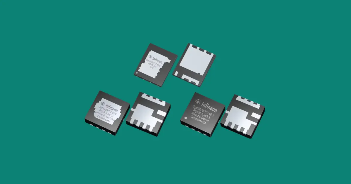
The portfolio balances on-resistance (RDS(on)), output charge (Qoss) and gate charge (Qg) to address conduction and switching losses. Infineon has also optimized the MOSFETs for 5 V gate drive, with support for switching frequencies beyond 1 MHz in suitable converter topologies.
Reduced Conduction and Switching Losses
Compared with the previous-generation OptiMOS 6 IQE013N04LM6CGSC, the new IQE010N04LM7CGSC reduces maximum RDS(on) by up to 33% at a gate-source voltage of 4.5 V. The figures of merit for output charge and gate charge are each reduced by up to 35%.
The devices are designed for gate-drive systems also used with GaN technology and support junction temperatures up to 175°C. Infineon offers source-down and dual-side cooling package configurations for applications with limited board space and demanding thermal requirements.
Source-Down and Dual-Side Cooling Packages
The IQE010N04LM7CG and IQE010N04LM7CGSC are available in PQFN 3.3 × 3.3 mm source-down center-gate packages, with overmolded and dual-side cooling options. Both devices have a maximum on-resistance of 1.0 mΩ at a gate-source voltage of 10 V.
The portfolio also includes three MOSFETs in PQFN 5 × 6 mm drain-down packages with dual-side cooling. The ISCH65N04LM7SC, ISCH69N04LM7SC and ISC011N04LM7SC offer maximum RDS(on) values of 0.65 mΩ, 0.69 mΩ and 1.1 mΩ respectively, also specified at 10 V gate drive.
The new OptiMOS 7 devices are intended for high-frequency power conversion in AI server and telecom equipment, including intermediate bus converters in both 48 V and emerging 800 V DC architectures.
Infineon's OptiMOS 7 40 V switching-optimized MOSFET portfolio is available in mass production.
Learn more and read the original announcement at infineon.com.
Technology Overview
Infineon's OptiMOS 7 40 V switching-optimized MOSFETs are designed for high-frequency DC-DC conversion in AI servers, data centers and telecom systems. Compared with a specified OptiMOS 6 predecessor, the portfolio offers up to 33% lower maximum on-resistance at 4.5 V gate drive and up to 35% lower output-charge and gate-charge figures of merit. The devices support 5 V gate-drive systems, junction temperatures up to 175°C and source-down or dual-side cooling PQFN packages.
FAQs
How do the new OptiMOS 7 40 V MOSFETs compare with OptiMOS 6?
Infineon reports up to 33% lower maximum RDS(on) and up to 35% lower output-charge and gate-charge figures of merit when comparing the IQE010N04LM7CGSC with its OptiMOS 6 predecessor. The on-resistance comparison is specified at 4.5 V gate drive.
What package and on-resistance options are available?
The 3.3 × 3.3 mm source-down devices offer 1.0 mΩ maximum RDS(on). Three 5 × 6 mm drain-down devices provide maximum values of 0.65 mΩ, 0.69 mΩ and 1.1 mΩ. These ratings are specified at 10 V gate drive.
Where are Infineon's switching-optimized OptiMOS 7 MOSFETs used?
The 40 V devices target high-frequency DC-DC conversion in AI servers, data centers and telecom infrastructure, including intermediate bus converters in 48 V architectures and low-voltage secondary stages of 800 V DC systems.
Related news
Keep up with the components and technology shaping electronics.
Join the club for member features, engineering discussion and easier access to the latest Component Club content.