Researchers Create New Gallium Oxide Semiconductor With Superior Current Capabilities
The Challenges of Gallium Nitride Semiconductors
Gallium nitride (GaN) has earned a strong reputation in power electronics, and for good reason. Its ability to switch at high frequencies while maintaining high efficiency has enabled power supplies that are significantly smaller and lighter than their silicon counterparts. Higher switching frequencies also allow designers to shrink inductive components, further reducing size and improving transient response.
Despite these advantages, GaN is not without its limitations. The most significant constraint by far is that, to date, commercially viable GaN devices are almost exclusively N-type. This limits design flexibility, particularly for CMOS-style switching architectures, where complementary P- and N-type devices are standard. N-type only devices also complicate high-side switching and the implementation of normally-off topologies, both of which are increasingly important in modern power electronics.
In practice, these limitations mean that while GaN can deliver impressive performance gains, circuit designers often have to work around its inherent constraints. The semiconductor’s strengths are clear, but fully exploiting them requires careful attention to topology and gate drive design. GaN is not a drop-in replacement for silicon; it demands a different approach, and the industry is still navigating the trade-offs.
Nagoya University Breakthrough: Stable P-Type Gallium Oxide Diodes
Gallium oxide (Ga₂O₃) has long been touted as a potential successor to silicon, silicon carbide, and even gallium nitride for power electronics. Its promise lies in higher voltage tolerance and better energy efficiency, but practical adoption has been stalled by a fundamental limitation: producing stable p-type layers. While n-type layers form reliably, the crystal structure of Ga₂O₃ resists the atoms needed for p-type conduction, leaving previous devices underperforming and limiting their commercial viability.
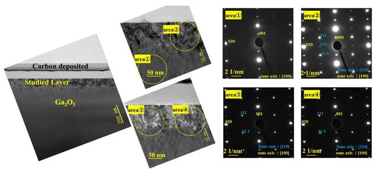 Image Credit: Shimizu et al., 2025
However, researchers at Nagoya University have now developed a process to reliably create p-type gallium oxide layers, enabling the first functional Ga₂O₃ pn diodes. Their method combines nickel ion implantation with a two-step annealing process: first at 300°C under a low-temperature plasma treatment and then at 950°C in oxygen. The procedure converts nickel into nickel oxide, properly integrating it into the gallium oxide lattice. The result is a pn diode capable of handling twice the current of previous Ga₂O₃ devices while maintaining energy efficiency far above conventional silicon-based diodes.
The implications of this new P-type semiconductor (and the resulting pn junction) are critical for its candidacy as a viable semiconductor. High-power systems, from electric vehicles to renewable energy inverters, stand to massively benefit from reduced energy loss, lower cooling requirements, and improved reliability. Unlike earlier experimental approaches, this method uses standard industrial equipment, suggesting the potential for scalable production.
This breakthrough in creating a p-type device addresses the main barrier that has kept gallium oxide largely theoretical for commercial power electronics. By overcoming the p-type challenge, Ga₂O₃ can now be considered a practical alternative to current semiconductor materials, promising both higher performance and lower operational costs in energy-intensive applications.
Could Ga₂O₃ Replace GaN?
It’s too early to declare gallium oxide a replacement for GaN, but the recent breakthrough is a crucial first step. Creating stable p-type layers enables true pn junctions, which have been the missing piece for practical Ga₂O₃ devices. With functional pn diodes, rectifiers and other power electronics can already operate more efficiently, reducing energy loss compared with previous Ga₂O₃ implementations.
That said, this technology remains in the developmental phase. GaN still dominates high-frequency and high-efficiency applications, and it will likely continue to do so for the foreseeable future. But the ability to form both n- and p-type layers opens a pathway for Ga₂O₃ to compete in areas where energy efficiency and high voltage handling are critical. Over the next decade, as processes mature and production scales up, gallium oxide could emerge as a viable alternative, or even a successor, to GaN in select applications.
You may also like