 Semiconductor packaging is becoming more demanding as devices combine multiple chips into a single module. Traditional photomasks are expensive and slow to change, especially when designs are updated frequently. Manufacturers need lithography tools that cut cost and allow faster iteration, while still hitting the precision targets set by advanced packaging.
Maskless digital lithography is one answer. Instead of relying on physical masks, light is projected directly onto a substrate, letting patterns be adjusted in real time. The result is flexibility, lower overhead, and the potential for higher yield.
A New Device from TI
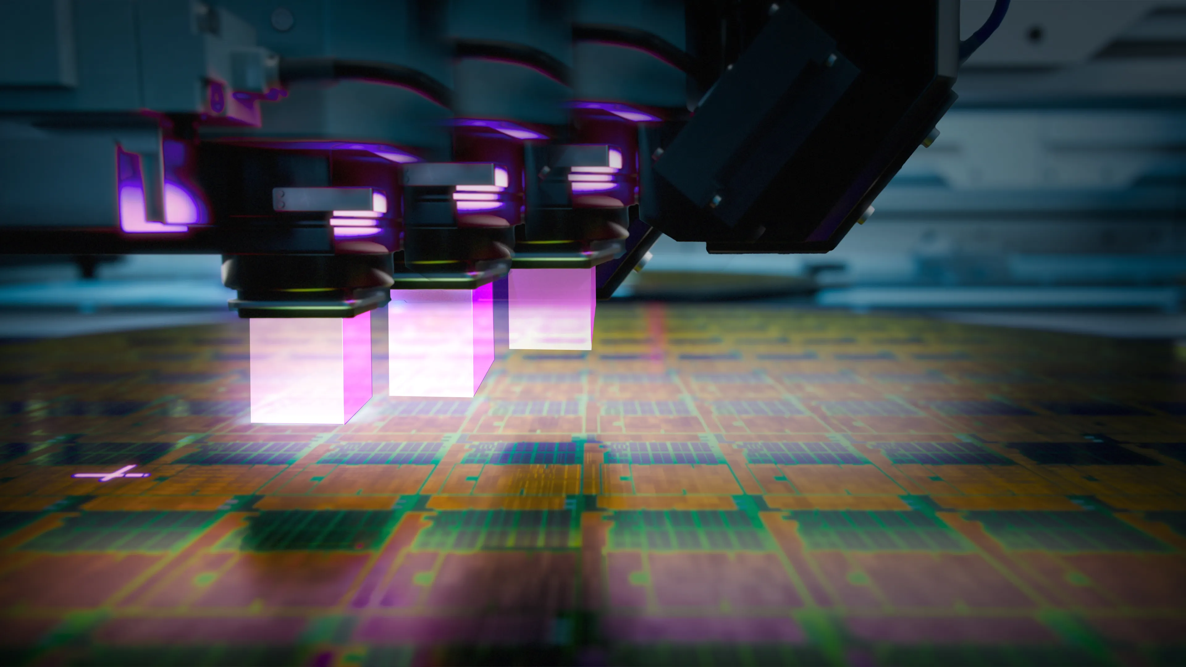
Texas Instruments has developed the DLP991UUV, a digital micromirror device designed specifically for this type of system. With 8.9 million mirrors operating as individually controlled pixels, the device reaches sub-micron resolution at data rates up to 110 gigapixels per second.
Each micromirror can shift to project part of a pattern, effectively turning the chip into a programmable photomask. Engineers can make design adjustments without retooling, a capability that reduces both cost and time.
The DLP991UUV also supports optical power levels of 22.5 W/cm² at 405 nm, and it can run at wavelengths down to 343 nm. Its 5.4 µm mirror pitch is the smallest in TI’s lithography line, enabling finer detail and more accurate patterning.
Why It Matters for Advanced Packaging
Advanced packaging is key for data centres, AI processors, and 5G systems, where higher bandwidth and lower power use are critical. Achieving that requires lithography tools that balance throughput and precision. By acting as a reprogrammable mask, the DLP991UUV provides a way to scale production while keeping yield high.
For engineers, the shift is practical. It means fewer defects, faster iteration cycles, and a chance to evaluate new designs without waiting for new masks to be fabricated. In industries where time-to-market is critical, those gains are significant.
Part of a Larger Trend
TI’s DLP technology has been used for years in projection systems and machine vision. The move into semiconductor manufacturing shows how the same principle, millions of tiny mirrors controlling light with precision, can reshape how chips are packaged and produced.
Learn more and read the original article on www.ti.com
Image credit: Texas Instruments
You may also like