The Challenge with Defects in Semiconductors
Of all industries on the planet, none are as technologically advanced as the semiconductor industry. Proof of this claim? Creating billions of transistors with features only a few hundred atoms across at scale reliably is an achievement that can’t even be fathomed by the human brain.
And yet, every year, engineers continue to push the limits of what can be done, with the smallest features still becoming smaller and smaller. However, as features continue to decrease in size, new problems quickly arise, and engineers must come up with solutions to those problems as fast as they can.
One such issue that semiconductor foundries face is tighter tolerances between layers, and this requires the use of extremely accurate imaging systems. Another issue that can crop up is the need for new deposition technologies that can provide uniform monolayers across extremely large areas.
But of all problems, the biggest by far facing engineers is defects in the wafer itself.
The purity of modern wafers used in semiconductors is unbelievable (well over 99.9999%), and yet, this still means that for any given chip, there will be defect areas on each die. These defects can be devastating to transistors, and considering that a design requires all transistors to work, a single defect can destroy a whole die.
While engineers can try to get around this with careful control and precision, they can also repeat designs across a die and turn off sections of a circuit that fail (such as some CPU manufacturers who have multiple cores on a single die, and only activate the ones that work).
But this still means that semiconductor dies can fail at times for unknown reasons, and trying to find these defects before manufacturing can be next to impossible. To make matters worse, defects that are atomic in size are virtually impossible to image directly, and this means that they are only discovered after a die has been manufactured.
Researchers create new method for visualising “mouse-bite” defects
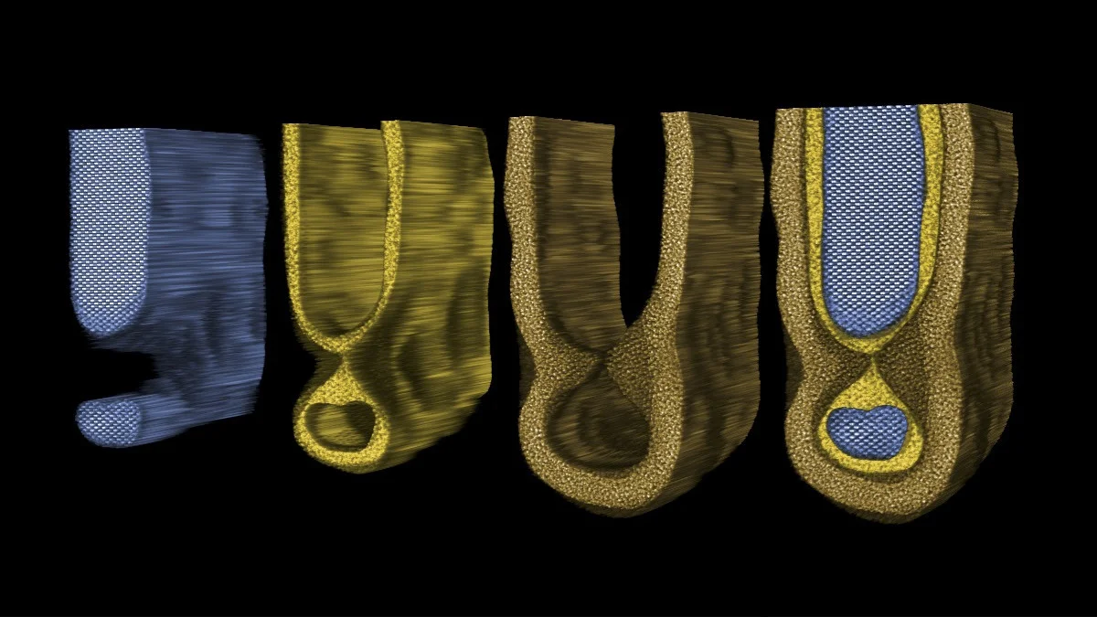
Recently, a research team at Cornell University in collaboration with Taiwan Semiconductor Manufacturing Company and Advanced Semiconductor Materials have developed a new high-resolution 3D imaging technique that can be used for debugging and fault-finding in computer chips, crucial for the development stage.
To image these defects, the team turned to electron ptychography, a computational imaging method, to image the interior structure of individual transistors. The researchers used the method to collect detailed scattering patterns of electrons after they pass through transistors. The result was an image with extraordinary clarity, revealing "mouse bites", the term for defects in the channel that result from the optimized growth process.
The researchers also discussed how the transistor has evolved from a flat and sprawling design to three-dimensional stacks as designers ran out of horizontal space. The study underscores how every atom's placement matters. The research showed the imaging capability that the new computational method provides, which could help to impact any device with a modern computer chip.
The new imaging method also has the potential to impact many modern electronics ranging from phones to quantum computing, and the ability to image tiny defects in semiconductors is something that the world has desperately needed for a long time.
How will these techniques help the future?
Trying to find defects in silicon wafers is next to impossible before a wafer is manufactured. Not only can defects crop up at any point in the process, but they are virtually invisible to the naked eye. Furthermore, as features enter the sub-1 nm realm, trying to find defects in wafers will only become harder.
However, if these defects can be imaged during development and fabrication, engineers will be able to identify where such defects occur, and potentially, identify the cause of the defects. This would allow semiconductor manufacturers to make changes to either their processes or the quality of wafers to improve yield rates in the future.
Such methods will also be essential for future devices that may struggle to have reasonable yield rates if defects are not avoided. Thus, not only will such techniques help with yield counts, but also reduce semiconductor manufacturing costs, any by extension, the price of cutting-edge silicon.
You may also like