 Recently, Samsung announced that it has broken the 10nm barrier currently facing DRAM, allowing them to pack more DRAM cells per unit area. What challenges does DRAM shrinking face, what did Samsung develop, and why is this innovation so critical now?
What Challenges Does Shrinking DRAM Face?
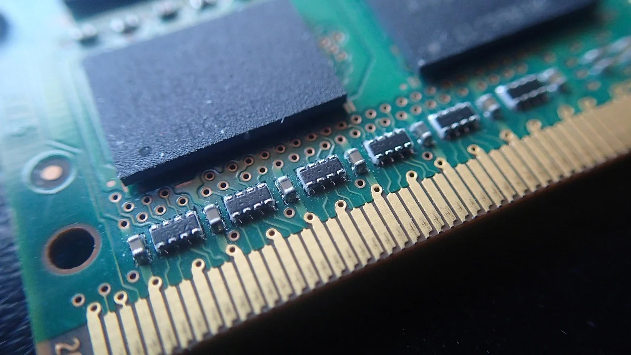
Of all technologies currently used in the field of computing, DRAM is arguably one of the most important. Everything from servers to mobile devices all require some kind of DRAM for use in fast storage that allows for immediate access to frequently used information. Unlike Flash and spinning disks, DRAM can hold data that can be loaded into the CPU for immediate use. Thus, DRAM allows for running programs to load code and data on demand, thereby eliminating the need for programs to fully exist in cache prior to execution.
However, while DRAM provides massive benefits, it also suffers from some drawbacks. One of these is that the amount of memory a machine can have is often very limited, with most RAM sticks topping out at 32GB. This low memory size combined with the large physical size of RAM means that machines which require considerable amounts will often have multiple slots (servers can have as many as 24 slots across 2 CPUs).
But the reason why DRAM sticks are so large, and why they have a maximum memory size comes down to how DRAM works. In order to store information, a DRAM cell consists of a capacitor and transistor, whereby the capacitor stores information as an electric charge on its plates, while the transistor is used to both charge and discharge this capacitor.
However, as the size of the capacitor directly relates to the amount of charge held to store a bit, as DRAM shrinks, the capacitors involved become smaller, reducing the amount of charge that can be stored. As such, reliably storing a charge on a DRAM cell becomes increasingly difficult, thus making it hard to produce reliable DRAM modules.
Because shrinking the capacitor is usually the limiting factor, in modern DRAM, the capacitor is often many times larger than the transistor that controls it. Advanced DRAM designs often employ deep trench or stacked capacitors to increase surface area without growing the chip footprint, but these methods become increasingly difficult below 20nm.
Therefore, the ability to further shrink DRAM cells is constrained by fundamental physics and manufacturing challenges related to the storage capacitor.
Samsung Breaks 10nm Barrier With Vertically Stacked 4F Transistor Configuration
Recently, Samsung announced that it has reportedly developed the world’s first sub-10nm DRAM working die, utilising its new “10a” process. While this doesn’t mean that Samsung is producing 10nm DRAM (as further research and development is still required), it does put Samsung ahead of other semiconductor manufacturers with regards to modern DRAM technology.
According to Samsung, the new process node is expected to scale to around 9.5~9.7nm, and advertises two main features. The first feature is the use of a 4F square cell structure, which is 30%~50% denser than traditional DRAM using 6F rectangular cells (3F x 2F). The second feature is the introduction of a Vertical Channel Transistor (VCT), which provides greater memory density, and better power efficiency compared to previous designs.
Samsung’s use of a 4F square cell (where F is the minimum feature size) allows each memory cell to occupy a smaller area compared to the conventional 6F rectangular cell. Traditional DRAM cells use elongated rectangles to accommodate the capacitor and transistor side by side. By shifting to a square layout and using vertical transistors, Samsung can stack elements more efficiently, resulting in a 30–50% increase in cell density.
This not only allows for more bits per chip but also reduces power per bit transferred, as shorter wiring and denser arrays reduce parasitic capacitances and resistances. In terms of materials, the new DRAM will utilise Indium Gallium Zinc Oxide (IGZO), which has already been demonstrated by Samsung back in 2018. By using IGZO instead of standard aluminium, the new DRAM will see less leakage, thereby improving data retention.
IGZO, a high-mobility oxide semiconductor, provides lower off-state leakage compared to traditional silicon-based transistors. This is particularly important in scaled-down DRAM cells, where leakage can quickly drain the stored charge from the tiny capacitors. The improved data retention and reduced leakage enable the use of smaller capacitors without sacrificing reliability, which is crucial for advancing to sub-10nm nodes.
Samsung expects to complete the development of 10a DRAM technology by the end of this year, and plans to launch mass production of the new devices in 2028. Additionally, Samsung has three more generations of DRAM in their roadmap, including 10b and 10c, after which they will move to 3D DRAM in the 10d generation, expected to be around 2029 ~ 2030.
Interestingly, other semiconductor companies such as Micron have stated that they won’t be following the 4F path, opting for 3D DRAM instead, as DRAM scaling with 4F presents numerous issues. However, as the DRAM market looks to double its capacity over the next decade due to the increasing importance of AI, it is likely that many semiconductor manufactures will rush to meet this demand.
Why is this Innovation So Critical Now?
The explosion of AI workloads, particularly large language models and machine learning training, has driven unprecedented demand for both processing power and memory. Modern AI accelerators, such as GPUs and custom ASICs, require vast amounts of high-speed DRAM to operate efficiently.
The resulting competition for RAM has led to significant shortages and price increases across consumer and enterprise markets. By increasing DRAM density per chip, Samsung’s technology can enable larger memory pools in smaller physical spaces, making it easier to build servers and AI systems with the massive RAM capacity these applications require. Furthermore, higher capacity DRAM chips can help enable new memory architectures such as unified memory, where both processors and accelerators access the same shared pool of RAM. This reduces the need for separate memory subsystems, streamlining data movement and potentially improving system efficiency, as seen in Apple’s recent hardware designs.
In the future, such high-density DRAM could even allow RAM to serve as a high-speed file cache or persistent memory layer, especially if paired with backup batteries or non-volatile enhancements to preserve data during power loss.
As software and AI requirements continue to grow, the limitations of current DRAM densities become more acute. Engineers, system designers, and cloud providers are all seeking ways to add more memory to their machines without increasing physical size or cost.
While it remains uncertain exactly when next-generation DRAM will reach mainstream deployment, since development and mass production are multi-year endeavors, these innovations represent a critical step toward addressing the industry’s memory bottlenecks.
You may also like