Lattice Launches Mach-N2 FPGAs with Post-Quantum Security and 16 Gbps SerDes
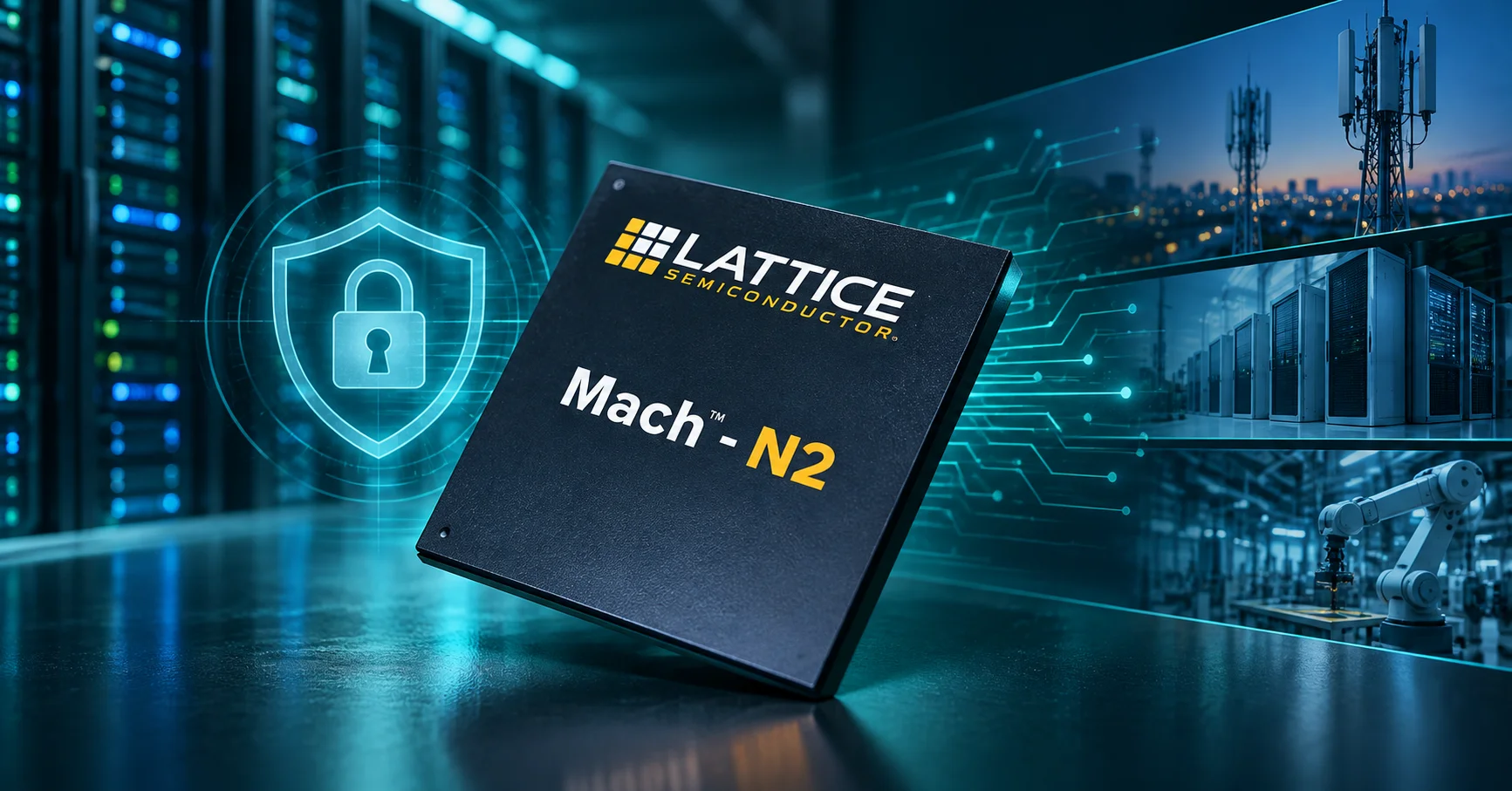 Lattice Semiconductor has introduced the Mach-N2 FPGA family, extending its secure control portfolio with devices designed for system control and security alongside modern processors and SoCs.
Built on the Lattice Nexus 2 platform, Mach-N2 scales from 65k to 220k system logic cells, with up to 12 Mb of embedded memory and 520 18 x 18 multipliers. The family adds integrated non-volatile flash, a hardware Root of Trust and high-speed connectivity including PCIe 4.0, 10G Ethernet and SerDes operating at up to 16 Gbps.
Lattice is targeting the devices at always-on functions such as system monitoring, power sequencing and system management in compute, communications and industrial infrastructure.
Post-Quantum Security Built into the FPGA
Security is a major part of the Mach-N2 architecture. The Root of Trust device supports CNSA 2.0-compliant post-quantum cryptography, including ML-DSA, LMS and XMSS for authentication and ML-KEM for key exchange.
Lattice has also built crypto agility into the platform, allowing cryptographic algorithms to be updated in the field as security requirements change, with anti-rollback protection intended to prevent systems reverting to an older implementation.
A Physically Unclonable Function (PUF) can be used to derive device identity, with support for DICE and SPDM attestation. Conventional cryptography includes AES-256-GCM bitstream encryption alongside ECDSA and RSA authentication. The architecture also supports anti-tamper monitoring with programmable responses.
Integrated Flash Supports Secure, Fast Boot
Mach-N2 stores configuration and data in on-chip non-volatile flash rather than relying on external configuration storage. Lattice says keeping the configuration bitstream on the FPGA protects it from physical access while enabling single-chip boot in under 30 ms.
The devices can store up to three configuration images, comprising primary, secondary and golden images. This gives system designers options for recovery if a configuration update fails or another image becomes unusable.
Fast configuration also fits the FPGA's role as an always-on system controller. Lattice describes Mach-N2 as supporting first-on, last-off system protection, allowing the FPGA to perform control and security functions around the rest of the system during power-up and shutdown.
High-Speed Connectivity for System Control
Mach-N2 adds SerDes bandwidth of up to 16 Gbps alongside PCIe 4.0 and 10G Ethernet, providing direct connectivity to processors, SoCs and other high-speed devices.
Lattice highlights network switches as one example, where the FPGA can aggregate control signals over PCIe and offload real-time monitoring and management of SFPs from the network CPU. Another use case is securing the data path, with support for in-line 10GbE encryption and decryption, secure key exchange with a processor and secure key storage and updates.
The Mach-N2 family is available to order now, with samples already shipping. The devices are supported by Lattice Radiant design software and the newly released Lattice Prompt AI-assisted FPGA development tool.
Learn more and read the original announcement at latticesemi.com.
Technology Overview
Lattice Mach-N2 is a family of Nexus 2-based secure control FPGAs scaling from 65k to 220k system logic cells. The family combines integrated non-volatile flash, hardware Root of Trust and post-quantum cryptography with PCIe 4.0, 10G Ethernet and SerDes connectivity up to 16 Gbps.
FAQs
What is Lattice Mach-N2?
Mach-N2 is a family of secure control FPGAs designed for system management, monitoring and security functions in compute, communications and industrial systems.
What post-quantum cryptography does Mach-N2 support?
The Root of Trust device supports ML-DSA, LMS and XMSS for authentication and ML-KEM for key exchange, alongside crypto agility for field updates.
How large are the Mach-N2 FPGAs?
The family ranges from 65k to 220k system logic cells, with the largest device providing 12 Mb of embedded memory and 520 18 x 18 multipliers.
You may also like