
 Image credit: onsemi (https://www.onsemi.com/company/newsroom/news-and-insights/onsemi-introduces-the-embedded-power-platform-a-breakthrough-architecture-for-the-ai-era)
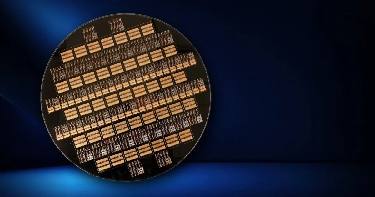
Power semiconductor development normally focuses on the device itself, but the package surrounding that device also affects electrical and thermal performance. onsemi is taking that idea considerably further with its new Embedded Power Platform (EPP), which uses silicon as the foundation of the package and embeds multiple semiconductor dies within a wafer-level architecture.
EPP can integrate silicon, silicon carbide (SiC) and gallium nitride (GaN) technologies, with devices including FETs, drivers and controllers embedded within a single package. Rather than treating electrical, thermal and mechanical design as separate stages, the platform is intended to allow these characteristics to be evaluated and optimized together.
The interesting question is what moving more of the power system into the package can achieve.
Moving Beyond the Conventional Power Package
One of the important changes is how devices within EPP are interconnected.
The platform replaces conventional wire bonds with wafer-level redistribution layers (RDLs). According to onsemi, this reduces parasitics and improves electrical performance. Instead of packaging individual devices and then connecting them at board or module level, multiple dies can be embedded and interconnected within the same silicon-based structure.
This also makes EPP a heterogeneous integration platform rather than a new type of monolithic power IC. Different semiconductor technologies can be incorporated into the architecture according to the requirements of the power system. The initial material specifically identifies silicon, SiC and GaN, alongside drivers and controllers.
Thermal design is brought into the same process. EPP is designed so that electrical, thermal and mechanical characteristics can be considered together rather than optimizing the semiconductor and then addressing packaging and thermal requirements separately. The silicon-based structure itself therefore becomes part of the electrical and thermal design.
That distinction is important. EPP is not simply putting more functions into a smaller package. It changes the level at which those functions are interconnected and optimized.
How Much Difference Can Integration Make?
onsemi is making some substantial performance claims for the platform. At the overall platform level, it says EPP can achieve between three and five times higher power density than current solutions, depending on the application. These figures are not a universal specification for EPP, and the results presented so far relate to particular implementations.
One example is a solid-state circuit breaker developed for AI infrastructure. The early EPP-based design was approximately 50% smaller and 20% cooler than the existing design used for comparison. onsemi attributes this partly to reducing packaging overhead and using the EPP footprint for heat conduction.
A second example comes from electric vehicle traction inverters. Here, the company reports up to four times higher power density and 15% lower power losses compared with conventional approaches. It is also developing the architecture so that a common inverter platform could be scaled across different vehicle power levels.
These examples are useful because they put numbers against the concept, but they also show why the headline performance figures need context. A 50% size reduction in the circuit-breaker design does not mean an EPP implementation will automatically halve the size of another power system. Likewise, the traction-inverter figures describe that application rather than an inherent fourfold improvement provided by the platform.
Bringing Packaging into Wafer Manufacturing
EPP uses onsemi's existing 12-inch silicon wafer manufacturing capability, with key integration processes performed within the semiconductor fab.
This is another distinction from treating EPP purely as an advanced package added after semiconductor fabrication. The package and its interconnections are part of the platform being designed and manufactured at wafer level. There is already an automotive evaluation underway. Subaru is receiving early access to EPP engineering samples, simulation models and technical expertise while assessing the technology for future electrified vehicle architectures. At this stage, that is an engineering evaluation rather than confirmation of EPP for a production vehicle.
Initial EPP sampling is expected during 2026 with strategic customers and ecosystem participants across automotive and AI applications.
Is the Package Becoming Part of the Power Architecture?
EPP is still a platform in the early stages of customer evaluation, and the performance figures released so far come from its developer. What has been demonstrated is the architecture: multiple semiconductor dies embedded in a silicon-based wafer-level structure, heterogeneous integration of silicon, SiC and GaN, and electrical, thermal and mechanical design brought together within the same platform.
Rather than designing the power device first and treating the package primarily as the structure around it, EPP brings packaging and interconnection into the power-system design from the outset.
Whether the performance gains demonstrated in the first applications translate across a wider range of systems will become clearer as engineering samples move into customer designs.
EPP therefore offers an early example of what happens when packaging and interconnection are treated as part of the power-system architecture rather than as separate considerations around the semiconductor.
You may also like