
Alphawave Semi Brings UCIe 3D Chiplet IP to TSMC’s 3DFabric Platform
Alphawave Semi tapes out UCIe 3D IP on TSMC’s SoIC-X 3DFabric, offering 10× power efficiency and 5× signal density for AI and HPC chiplet designs.
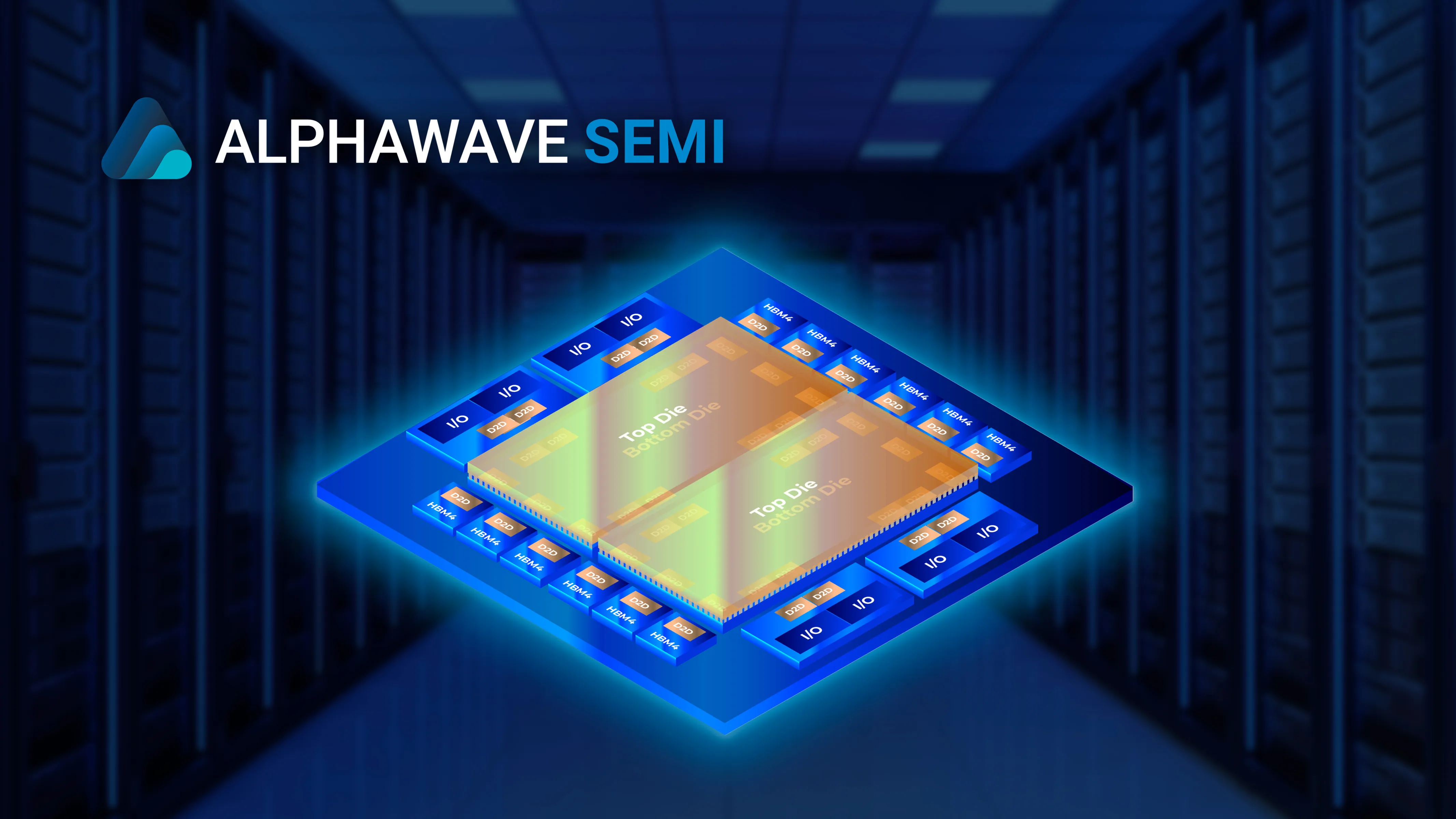
UCIe has become the standard for die-to-die connectivity. Most implementations so far have used 2.5D approaches, where dies are placed side by side on an interposer. Alphawave Semi’s latest development demonstrates UCIe operating in a true 3D stack.
What Alphawave Has Announced
Alphawave Semi has completed tape-out of its UCIe 3D IP using TSMC’s SoIC-X technology, part of the 3DFabric platform. The design uses face-to-face stacking, with through-silicon vias providing power and ground connections between layers. In this example, a 5 nm die forms the base while a 3 nm logic die is bonded above it.
The company reports that the 3D UCIe link achieves up to ten times greater power efficiency and five times higher signal density compared with 2.5D solutions. Alphawave has also developed a design flow that simplifies construction and verification of these stacks, aiming to reduce one of the key barriers to adoption.
Why It Matters for AI and HPC
AI and HPC systems often face limitations not from raw processing power but from the cost of moving data between chips. Shorter vertical connections cut the energy per bit and increase available bandwidth within the same package footprint. The result is higher performance per watt, which is particularly valuable in data centre and supercomputing environments.
Thermal management is still a significant challenge for 3D stacks, since heat from multiple dies builds up in a smaller space. Alphawave’s work with TSMC and Siemens indicates that the focus is not only on boosting performance but also on ensuring that these designs can be manufactured and verified reliably at scale.
Industry Collaboration
The project combined Alphawave’s UCIe IP with Siemens’ design and verification tools and TSMC’s SoIC-X manufacturing platform. It highlights the way ecosystem partners are working together to make 3D integration practical for production. Both UCIe and advanced packaging are likely to remain central to how the industry pushes performance further for AI and HPC.
Learn more and read the original article on www.awavesemi.com
Related news
Keep up with the components and technology shaping electronics.
Join the club for member features, engineering discussion and easier access to the latest Component Club content.