
Samsung HBM4 Ships At 11.7Gbps And 3.3TB/s Per Stack
Samsung begins mass production of HBM4 delivering 11.7Gbps per pin and up to 3.3TB/s per stack with 4nm logic base die, 2,048 I/Os, and improved power efficiency for AI datacenters.
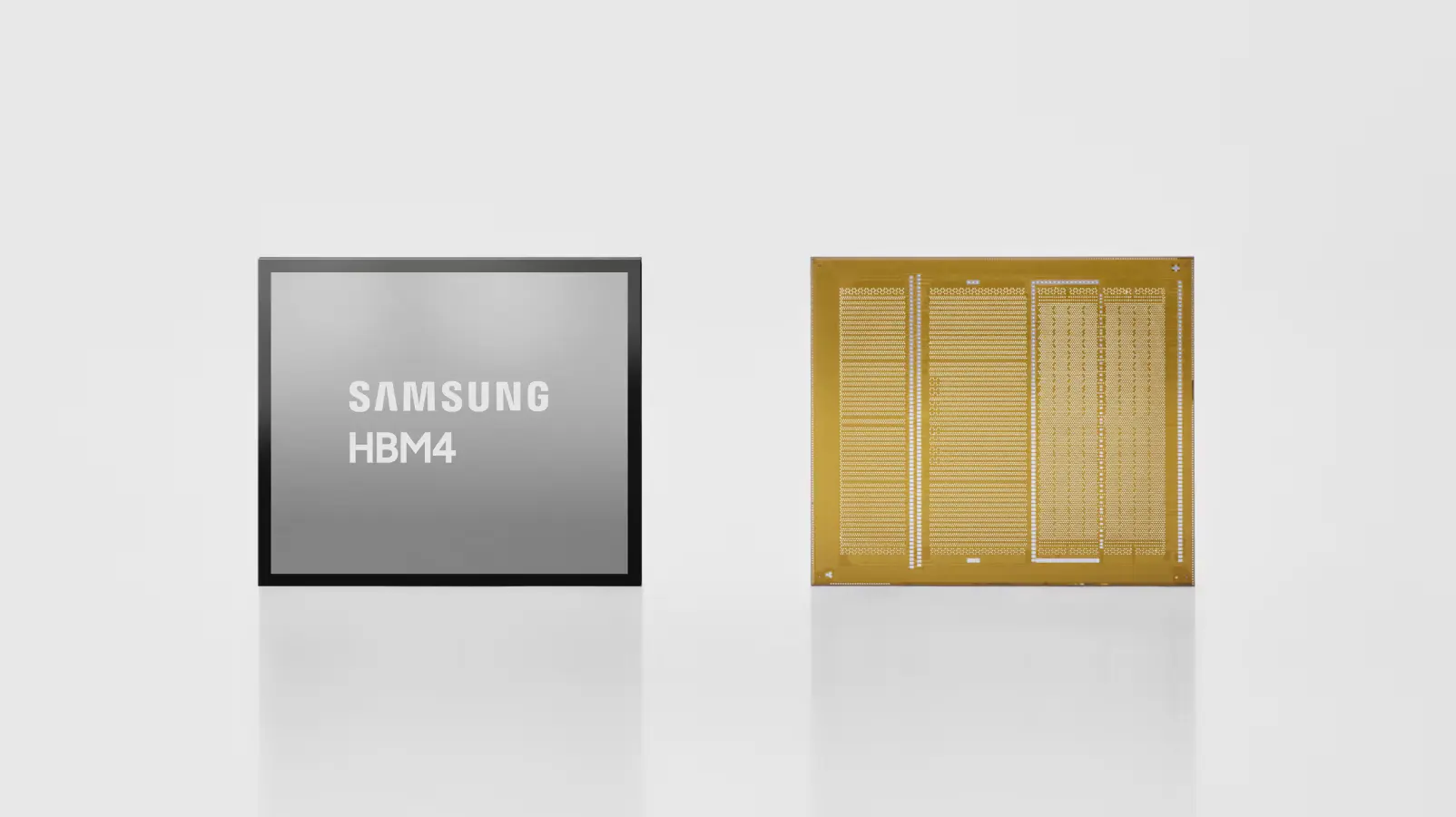
11.7Gbps Baseline With Headroom To 13Gbps
HBM4 operates at a consistent 11.7Gbps transfer rate, with capability extending toward 13Gbps under appropriate conditions. That moves well beyond the 9.6Gbps ceiling of HBM3E and shifts the memory subsystem closer to where next-generation AI accelerators need it. The increase is not incremental. As pin counts double from 1,024 to 2,048, signal integrity and timing margins become more difficult to preserve across stacked dies and interposers.
Per-stack bandwidth reaches up to 3.3TB/s, roughly 2.7 times that of HBM3E. In real systems this changes how many stacks are required to saturate a GPU complex. Fewer stacks per package can reduce routing complexity and interposer real estate, though thermal density increases accordingly.
4nm Logic Base Die And 1c DRAM Process
Samsung moves to a 4nm logic base die for HBM4 while using its 6th generation 10nm class DRAM node. The logic base die handles signal routing and control functions that increasingly resemble SoC behavior rather than passive stacking. Shrinking that logic node is not just about speed. It reduces power overhead associated with managing twice the I/O count.
Stacking remains at 12 layers for capacities between 24GB and 36GB, with 16-layer configurations extending toward 48GB. As stacks grow taller, through-silicon via density and vertical resistance become more influential in both latency and thermal gradients.
Power Delivery And Thermal Control Under 2,048 I/Os
Doubling I/O count raises switching activity and current distribution demands. Samsung integrates low-voltage TSV structures and power distribution network optimization to manage those effects. Power efficiency is improved relative to HBM3E, and thermal resistance sees measurable gains. Heat dissipation is addressed not just through packaging but through architectural adjustment at the core die level.
In large AI clusters, these differences show up as sustained throughput stability rather than peak benchmark figures. Memory subsystems that throttle under heat negate bandwidth gains on paper. The challenge is keeping stacks stable while maintaining tight pitch and dense stacking.
Production Scale And HBM Roadmap Direction
Samsung has moved this generation directly into mass production rather than extended sampling. Coordination between foundry and memory processes plays a role here, particularly with design technology co-optimization between the 4nm logic base and DRAM stacking. Scaling output capacity matters because AI accelerator vendors cannot redesign around constrained memory supply.
HBM4E sampling is already on the horizon, alongside custom variants aligned with ASIC development cycles. That cadence suggests that memory bandwidth growth will continue tracking AI model expansion rather than slowing. Compute density is still rising. Whether packaging and thermal systems can keep pace remains the open question.
Learn more and read the original announcement at www.semiconductor.samsung.com
Related news
More from Samsung
Keep up with the components and technology shaping electronics.
Join the club for member features, engineering discussion and easier access to the latest Component Club content.