 Power electronics inside AI data centers, grid infrastructure, and industrial electrification systems are increasingly running into a familiar constraint. Switching devices may offer the voltage rating and efficiency designers want, yet the packaging around them starts to become the real limitation. Heat has to go somewhere. Clearance inside power racks keeps shrinking. Even mechanical height can quietly dictate how much power a rack can realistically deliver.
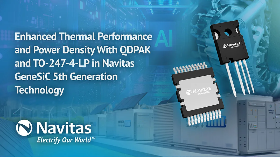
Navitas has introduced two new package options built around its fifth-generation GeneSiC silicon carbide MOSFET platform that try to tackle those constraints directly. The devices target 1200 V power stages used in high-density energy systems, but the changes here are not really about the silicon itself. Most of the attention has shifted to how that silicon integrates thermally and mechanically into real hardware.
Fifth-Generation GeneSiC MOSFET Technology Under the Package
The devices are built on Navitas’ Trench-Assisted Planar silicon carbide MOSFET structure, a design approach that attempts to balance switching efficiency with predictable gate behavior. Silicon carbide switching stages often push designers into uncomfortable territory where parasitic turn-on and unstable gate behaviour appear at exactly the worst moment, usually when currents are highest.
Navitas reports that this generation improves the RDS(on) × QGD figure of merit by roughly thirty five percent. The QGD to QGS ratio also drops by about a quarter, which matters more than it might first appear. Gate charge dynamics are one of those quiet parameters that determine whether a switching transition behaves cleanly or starts producing ringing that takes half a board revision to tame.
Threshold voltage also remains relatively high. With VGS(th) above three volts, the devices are less likely to experience unintended turn-on during fast switching events. Anyone who has spent time probing a half bridge at several hundred volts will recognise how valuable that stability can become.
Top-Side Cooling Changes How Heat Leaves the Device
One of the more interesting additions is the QDPAK package with top-side cooling. Conventional surface-mount power packages normally rely on thermal paths that flow through the PCB, which inevitably forces designers to dedicate significant copper area simply to carry heat away from the device.
QDPAK flips that thermal path. Heat exits through the top of the package directly into a heatsink rather than into the board. That sounds simple, but the mechanical consequences ripple through the entire design. Thermal bottlenecks shift away from copper layers and toward the heatsink interface, which in many systems is easier to control.
The package footprint is relatively compact at roughly fifteen by twenty-one millimetres, with a height just over two millimetres. Creepage distance extends to about five millimetres using a molded groove in the package body, helping it remain suitable for high-voltage designs without expanding the overall footprint. The molding compound itself carries a comparative tracking index above six hundred, supporting use in high-voltage environments that would normally demand careful insulation planning.
Larger die sizes can also be accommodated in this package format. That allows very low on-resistance variants while keeping the assembly compatible with automated surface-mount production.
Low-Profile TO-247 Addresses Mechanical Height Limits
Through-hole power packages have never really disappeared from high-power systems, but the traditional TO-247 format often introduces its own mechanical headaches. The vertical height above the board can quietly interfere with airflow channels or enclosure constraints inside dense power assemblies.
Navitas has introduced a low-profile TO-247-4L version that attempts to reduce that height while maintaining the electrical behaviour engineers expect from the four-lead configuration. The asymmetrical lead structure separates the gate and Kelvin-source connections using thinner pins, which improves manufacturing tolerances and helps maintain cleaner gate drive paths on the PCB.
The format is aimed squarely at systems where vertical clearance becomes a limiting factor. AI data-center power shelves are one example, where every millimetre of available space tends to translate into additional power density.
Where These Devices Sit In Modern Power Architectures
The new MOSFETs remain within the familiar 1200 V silicon carbide class that already dominates many industrial and infrastructure converters. Two resistance options appear in each package family, roughly 6.5 milliohms and 12 milliohms, allowing designers to trade conduction loss against cost depending on current levels.
In practice the packaging changes may be more influential than the silicon improvements themselves. Power electronics designers often discover that thermal extraction, creepage management, and mechanical clearance drive layout decisions long before semiconductor limits are reached.
These packages are essentially an attempt to remove some of those mechanical barriers so the electrical performance of silicon carbide can actually be used.
Learn more and read the original announcement at www.navitassemi.com
You may also like