
India Launches First Advanced 3D Chip Packaging Plant
Recently, India announced its plans to launch its first advanced 3D chip packaging plant to push India’s rise in the semiconductor field. What challenges do traditional chips face, what is India doing, and why is this a great sign for semiconductor development?
The Challenges with Semiconductor Chips
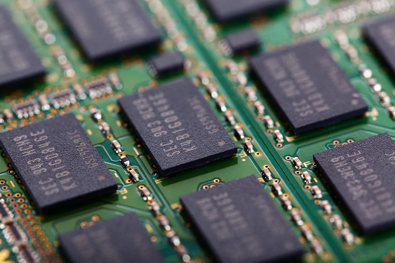
One of the biggest and most defining features of semiconductor chips is that they are planar, meaning they are primarily designed and manufactured in two dimensions. While transistors themselves are three-dimensional in structure, the vast majority of chips involve spreading transistors outward across the surface of a wafer, rather than stacking them vertically. Some devices do extend upwards, especially in the case of 3D NAND, but such designs are not the norm, and thus most devices are dependent purely on their square millimeter size.
It is this planar design that restricts the capabilities of modern chips, meaning that engineers are constantly looking at ways to improve their capabilities. One solution that is quickly becoming a reality is stacked chiplets, which take multiple planar devices, and stack them ontop of each other. Small gold interconnect wires are used to connect the different dies together, and this allows for extremely dense designs. Such designs can combine memory and processor into the same package, allowing for reduced power, increased speed, and reduced space.
But doing this type of manufacturing is no small feat, requiring highly specialsied facilities. As such, this industry is currently dominated by Western nations who have had decades of experience.
However, this is starting to change, and many nations around the world are investing in their own semiconductor foundries and packaging houses, including China, Taiwan, South Korea, Japan, and the US.
India To Launch New 3D Advanced Packaging Facility
In a major move, India recently launched its first advanced 3D chip packaging plant in Bhubaneswar, Odisha. This facility marks a major step for India's semiconductor ambitions, forming a core part of the India Semiconductor Mission (ISM), which aims to promote domestic semiconductor manufacturing and advanced packaging capabilities.
The project is being developed by a US-based company, 3D Glass Solutions Inc, through its Indian subsidiary Heterogeneous Integration Packaging Solutions Pvt Ltd (HIPSPL), and has received funding support from Intel Corporation and other investors. The foundation stone for the facility was laid by Odisha Chief Minister Mohan Charan Majhi and Union Minister for Electronics & Information Technology Ashwini Vaishnaw, with Intel CEO Lip-Bu Tan participating virtually.
The total investment for the project is approximately ₹1,934 crore (approximately $200 million), and when fully operational, the facility is projected to produce up to 70,000 glass panels annually, assemble 50 million units, and manufacture around 13,000 advanced 3D heterogeneous integration (3DHI) modules each year. These production targets will be achieved in phases as the plant scales up to full capacity.
The facility is expected to generate around 2,500 direct and indirect employment opportunities in the region, providing a boost to the local economy. Officials have described the project as a strategic shift for Odisha, moving the state's industry focus from traditional sectors like mining and metals toward high-tech electronics manufacturing and IT infrastructure.
The plant is anticipated to attract talent, foster innovation, and establish Odisha as a key player in India's growing electronics ecosystem.
How this Move Demonstrates the Importance of Semiconductor Sovereignty
India's establishment of an advanced 3D chip packaging facility is a serious step toward semiconductor sovereignty, with implications than will extend well beyond the obvious. By developing in-country capabilities for advanced packaging, India is reducing its reliance on foreign suppliers for critical stages of semiconductor production, helping to secure its technology supply chain in an increasingly competitive global environment.
Firstly, by India being able to produce such devices, not only is it cementing itself to become independent on semiconductor technologies in the future, but it is securing its supply chain. While it is possible for a nation to make semiconductors, being able to package them is another thing entirely. For example, India could source wafers and dies directly, then use its advanced packaging solutions to create powerful devices without needing bleeding edge technologies.
Secondly, even if India cannot get access to wafers or dies, it could still combine older generations of memory and CPU technologies in the same package. While this would not necessarily result in devices that are more powerful than current market leaders, it does provide a path for India to integrate existing technologies into new system-on-chip (SoC) or system-on-module (SoM) solutions tailored for domestic and regional needs, potentially improving performance per cost or enabling applications that would otherwise require costly imports.
Thirdly, by moving to chiplet designs, chip yields can be massively improved as dies can become smaller (fewer transistors, and thus, fewer failure points). Designs can also be segregated to make them easier to operate, and the need for large dies with billions of transistors can be eliminated. Thus, instead of needing the latest node with the most number of transistors, a few stacked dies with fewer transistors can have more transistors in a given package. This modular approach not only improves manufacturing yields and flexibility but also enables faster time-to-market for customized solutions, making the domestic industry more agile and competitive.
Overall, when this facility gets into operation, we will likely see some exciting developments coming out of India. The plant’s success could pave the way for further investments in advanced semiconductor technologies, accelerate the growth of India’s electronics sector, and contribute to the country’s aspirations to be a global technology leader. It will also serve as a model for other emerging economies seeking to increase their technological self-reliance.
Related news
More from Robin Mitchell
Keep up with the components and technology shaping electronics.
Join the club for member features, engineering discussion and easier access to the latest Component Club content.