Samsung First to Build 3D Stacked Transistors
Finally, it looks like that we may be entering the next era of semiconductor design, utilizing stacked transistor designs. Samsung has just announced that it is the first to achieve a 3D stacked design that could instantly double the number of devices on a die, and if their claims are true, could be a game-changer for the industry and technology as a whole.
Samsung Announces Stacked Transistor Design
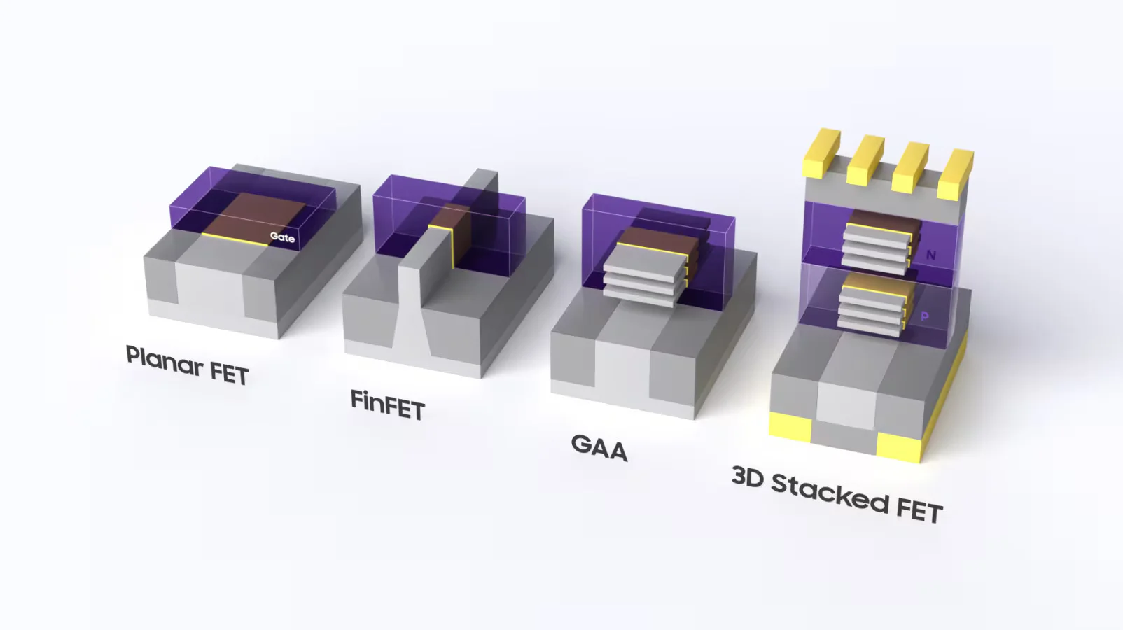
Recently, during the 2026 VLSI Symposium, Samsung Electronics announced the world’s first 3D Stacked Field Effect Transistor (3D Stacked FET), winning the Best Paper award. The development of the new technology, according to Samsung, not only puts the company ahead of its competitors, but will likely lead to vertically integrated logic semiconductors.
While traditional semiconductor technologies have focused on reducing the size of transistors to increase their count (and thus improve computational capabilities), the new technology developed by Samsung instead stacks transistors vertically. This technology, if deployed, could instantly see devices with twice the transistor count as compared to current devices on the market.
According to Samsung, the new technology, which is still in its early days, has already demonstrated an array of impressive achievements. For example, the 3D technology has been stated to have a 42 nm gate pitch, which is smaller than the current industry leader (having a gate pitch of 48 nm). Additionally, Samsung also claimed that the 3D technology developed by their team is the smallest transistor gate pitch ever demonstrated, and that the technology will play a critical role in future logic devices.
Additionally, the new design also utilizes a multitude of world’s first features, including three nanosheet channel tiers on both the upper and lower transistors, and a direct vertical RX Bounded Contact (RBC) connection.
Moving forward, Samsung noted that now that they have proven the concept, they will continue to work towards commercializing the new technology. According to Samsung, this technology will not only help to benefit AI and HPC (High-Performance Computing), but will also enable for improved energy efficiency, something that is increasingly becoming more important in modern electronics. As such, it is believed that this technology will be ideal for applications requiring low-power operation.
Why is this Development So Important?
To say that this announcement is important is the understatement of the century. Ever since the development of the first integrated circuits, engineers have relied on a single mechanism to make chips better: transistor size.
By shrinking transistors, it becomes possible to fit more of them onto a given area, and this leads to increased memory sizes, accelerator capabilities, and higher CPU frequencies. However, transistors have never been stacked before in logic designs, and the moment transistors can be stacked, everything changes.
The first advantage that comes from stacking transistors is that it instantly doubles the number of devices on a given die. However, this advantage quickly snowballs when considering that if one layer of transistors can be grown, then growing additional layers should become trivial. With two layers, four times the number of transistors can fit, and from there, it doesn’t take a leap of imagination to see how many more devices can be packed into a die. More layers means more active parts, which directly translates to massively increased memory densities and CPU capabilities.
But the advantages of 3D transistors go far beyond density. Another potential advantage to 3D transistor designs is that it allows for older tech nodes to be used. Currently, modern transistor designs require tight spacing between different layers, and this makes it difficult to produce high-end devices using older technologies. However, if a 3D transistor stack uses an older node that has larger spacing between layers, then not only does that technology become easier to produce, but also cheaper. As such, we could see complex devices being made using cheaper nodes and processes, while also seeing significantly higher yields (as less goes wrong during the manufacturing process).
Additionally, there is also the possibility that 3D stacked transistors could provide increased switching speeds. Simply put, transistors that are physically closer to each other will have reduced capacitive coupling, thus allowing gates to charge faster. At the same time, it may even be possible to have dedicated contacts between the various transistors, thus eliminating some of the parasitic capacitance between neighboring devices.
When Could this Technology Hit the Shelves?
It is not entirely clear when this technology will be available for mass production, but what is clear is that Samsung is definitely working towards getting it out there. Considering that SRAM is essentially the ultimate memory solution, it is likely that the first devices to utilize the new technology will be SRAM-based devices (such as caches).
However, it is likely that this new technology won’t be available commercially until the early 2030s. As most foundries are geared around planar devices, it will require years of testing, yield experimentation, and customer uptake to convince the industry that this new technology is worth it.
While it would be great to see these devices in mobile and consumer applications, the reality is that consumer devices don’t need this kind of processing power right now. Instead, these devices are far more likely to end up in AI and datacenter markets, and even then, it is possible that the AI bubble will pop before these devices hit the shelves.
All we can do now is wait and see what happens. If this technology is able to deliver on its promise, it could very well usher in a new era of computational devices.

Related news
More from Robin Mitchell
Keep up with the components and technology shaping electronics.
Join the club for member features, engineering discussion and easier access to the latest Component Club content.