Beyond SiC and GaN: Researchers push semiconductors past 7 eV
Researchers have made silicon-doped α-(AlGa)₂O₃ conductive at bandgaps above 7 eV, opening up an extreme end of semiconductor physics that until recently looked far more like insulation than electronics.
There is a problem with pushing semiconductor bandgaps ever wider. The same properties that have made SiC and GaN so useful for power electronics become increasingly attractive as the bandgap grows, but eventually there comes a point where getting current through the material becomes difficult in the first place.
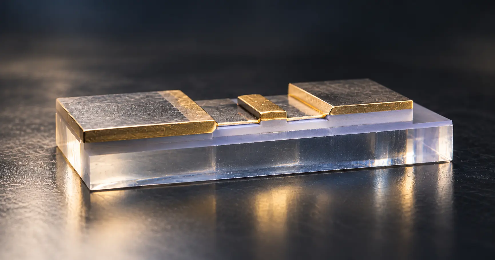
Researchers led by Cornell University have now pushed that boundary beyond 7 eV using silicon-doped alpha aluminum gallium oxide, or α-(AlGa)₂O₃. The films, reported in Nature on October 7, remain conductive despite having bandgaps greater than 7 eV. The team has also used the same material family to make a Schottky diode and a field-effect transistor called the AlphaFET.
That second part makes the work particularly interesting. There is a large difference between growing an exotic material with an impressive bandgap and showing that charge can actually be controlled well enough to make an electronic device from it.
When a wider bandgap stops being useful
Silicon has a bandgap of about 1.1 eV. Move to 4H-SiC and it rises to roughly 3.3 eV, while GaN sits around 3.4 eV. Those wider bandgaps are closely tied to the high electric fields these materials can withstand, one of the reasons they have become so important in power conversion.
The attraction of going wider is easy to see. The Baliga figure of merit, commonly used when comparing semiconductor materials for power devices, has a very strong dependence on bandgap. In the new paper, the researchers point to a relationship proportional to bandgap raised to the power of 5.5.
Unfortunately, bandgap is not a specification that can simply be turned up indefinitely.
A semiconductor still needs mobile charge carriers. These are normally introduced in controlled amounts through doping, but that becomes harder as the bandgap increases. Go wide enough and a material that looks exceptional on a chart can become extremely difficult to turn into anything useful.
Back in 2021, Cornell had already shown that α-(AlGa)₂O₃ could be pushed across a huge bandgap range, from about 5.4 to 8.6 eV, simply by changing the aluminum-to-gallium ratio. But the further they pushed it, the less useful the material became electrically. Growing the crystal was no longer the main problem. Keeping enough carriers moving through it was.
That is where the comparison with sapphire becomes useful. Sapphire is aluminum oxide, and engineers normally value it precisely because it does not conduct. As α-(AlGa)₂O₃ becomes richer in aluminum, the challenge is stopping it from crossing the same line into electrically useless territory.
Getting current through a 7 eV material
The researchers used silicon as an n-type dopant and changed the way the α-(AlGa)₂O₃ layers were grown.
The latest films were produced using suboxide molecular-beam epitaxy, or S-MBE. Rather than supplying all of the constituent elements in their conventional form, the process uses pre-oxidized molecular beams during growth. Combined with a carefully arranged series of buffer layers, it produced a dramatic improvement in conductivity.
In the colossal-bandgap region above 6 eV, the team reports room-temperature conductivity more than 100 million times higher than previous results. Crucially, that improvement continued into material with a bandgap exceeding 7 eV.
The transistor itself needs a little more explanation because the headline number can otherwise be misleading. Public conference material from the researchers describes the AlphaFET as using a silicon-doped α-(Al₀.₅₁Ga₀.₄₉)₂O₃ channel with a bandgap of 6.7 eV, rather than the greater-than-7 eV material used for the highest-bandgap conductivity result. The group also fabricated Schottky diodes from the material system.
So this is not quite a “7 eV transistor,” even though the wider material has now been made conductive. It is still, according to the researchers, the widest-bandgap semiconductor in which controlled carrier transport and field-effect device operation have been demonstrated.
That is a more useful milestone than the 7 eV number on its own. Materials sitting this far beyond SiC and GaN are beginning to show behavior that can be used in actual electronics, even if the devices themselves are still laboratory prototypes.
A long way from replacing SiC
There is another practical detail in the work that deserves attention. The α-(AlGa)₂O₃ layers are grown on sapphire, rather than on a small and difficult-to-produce exotic substrate.
Cornell's earlier work found that the orientation of the sapphire is critical. Using the m-plane allows the alpha phase to remain stable as aluminum is added, while other orientations encourage the material to move into narrower-bandgap phases.
Sapphire is attractive for another reason too: large, high-quality wafers are already widely available. That does not make the rest of the process easy, but at least the substrate is not an exotic material that would require an entirely new manufacturing supply chain.
The AlphaFET is still nowhere near a commercial SiC MOSFET or GaN HEMT. Carrier mobility may prove limiting, while contacts, interfaces, thermal performance and long-term reliability all still need work. Then there is the much harder question of whether the material can be grown and processed consistently enough for real manufacturing. A huge bandgap only gets you part of the way.
What has changed is the point at which that discussion can begin. A few years ago, the team had shown that α-(AlGa)₂O₃ could be grown across an enormous bandgap range. Now it has shown that useful conductivity can survive beyond 7 eV, while active devices are already operating at 6.7 eV.
For power electronics, that opens up a part of the materials map that until recently looked much more like the territory of insulators than semiconductors.
Related news
Keep up with the components and technology shaping electronics.
Join the club for member features, engineering discussion and easier access to the latest Component Club content.