Renesas Chiplet SoC Tech for Automotive SDV ECUs
Renesas develops automotive SoC technologies for SDV-era multi-domain ECUs, combining chiplet safety across UCIe, expanded AI NPUs, and advanced multi-domain power control.
Extending Functional Safety Across Chiplets
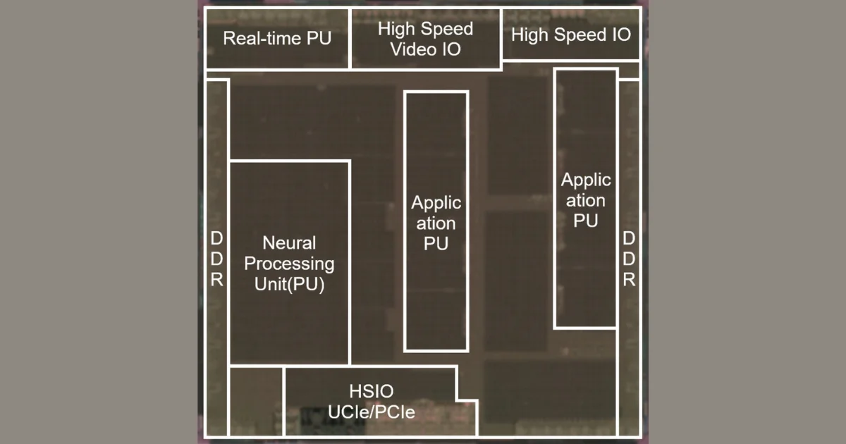
Scaling an SoC across chiplets is straightforward until safety requirements enter the picture. Automotive systems targeting ASIL D cannot tolerate uncontrolled resource interference between domains. Renesas combines the UCIe die-to-die interface with a proprietary RegionID mechanism that propagates isolation context across chiplet boundaries. Conventional UCIe links do not natively transport those identifiers. Renesas maps RegionIDs into physical address space and encodes them for transfer across the interconnect, allowing memory management units and real-time cores to enforce access boundaries across dies.
Bandwidth across that interface has been demonstrated at 51.2 GB per second, approaching intra-SoC transfer speeds. The point is not the raw number. It is that safety tagging does not become the throughput bottleneck. When multi-domain ECUs consolidate previously separate controllers, preserving isolation without throttling performance becomes a structural requirement.
Clock Architecture Under Expanding AI NPUs
AI accelerators inside automotive SoCs continue to expand in area. As neural processing units grow, clock latency between centralized generators and distant logic blocks increases. That latency complicates timing closure, especially at advanced nodes. Renesas restructures the clock architecture by dividing clock pulse generators into smaller sub-module level units. These mini generators reduce local latency but introduce complexity during validation.
Test clock synchronization is not optional in automotive silicon targeting zero-defect quality. Multiple clock layers increase the risk of phase misalignment during manufacturing test. Renesas integrates test circuitry directly into the hierarchical clock structure and unifies user and test clock paths so that phase alignment can be controlled under a single source during test mode. That adjustment does not change application performance. It changes manufacturability and yield confidence.
Power Domains, IR Drop, and Safety Monitoring
As process geometries shrink and performance climbs, current density rises. Large automotive SoCs now employ extensive power gating. Renesas reports over ninety power domains, enabling fine-grained control from milliwatt standby regions to blocks consuming tens of watts under load. Splitting power switches into ring structures and row structures distributes current more evenly. The ring switch suppresses inrush current during power-up. The row switch equalizes impedance once the domain is active. IR drop is reduced by roughly thirteen percent compared with conventional layouts.
Functional safety overlays that power control. Dual core lock step configurations operate with independent power switches and controllers so that failures can be detected without propagating silently. Loopback monitoring on each power switch gate ensures that OFF states are verified rather than assumed. Voltage supervision is handled by a digital monitor designed to resist temperature drift, improving aging tolerance at the millivolt level. These mechanisms do not advertise themselves in a block diagram. They appear when something goes wrong.
Architectural Direction for Multi-Domain ECUs
Software-defined vehicles compress what used to be separate control units into centralized computing platforms. Chiplet scalability allows larger compute resources without pushing reticle limits. AI accelerators expand to handle perception and fusion workloads. Power domains multiply to maintain efficiency. Safety boundaries must remain intact across all of it. The interaction between these elements determines whether consolidation simplifies the vehicle architecture or simply moves complexity into silicon.
Renesas is applying these technologies in its R-Car X5H SoC aimed at multi-domain ECUs. The architectural decisions reflect where automotive compute is heading rather than where it has been.
Learn more and read the original announcement at www.renesas.com
Related news
More from Renesas
Keep up with the components and technology shaping electronics.
Join the club for member features, engineering discussion and easier access to the latest Component Club content.